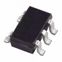
AD8051ARTZ-R2 Analog Devices Inc, AD8051ARTZ-R2 Datasheet

AD8051ARTZ-R2
Specifications of AD8051ARTZ-R2
Available stocks
Related parts for AD8051ARTZ-R2
AD8051ARTZ-R2 Summary of contents
Page 1
FEATURES High speed and fast settling 110 MHz, −3 dB bandwidth (G = +1) (AD8051/AD8052) 150 MHz, −3 dB bandwidth (G = +1) (AD8054) 145 V/μs slew rate 50 ns settling time to 0.1% Single-supply operation Output ...
Page 2
AD8051/AD8052/AD8054 TABLE OF CONTENTS Features .............................................................................................. 1 Applications ....................................................................................... 1 Pin Connections (Top Views) ......................................................... 1 General Description ......................................................................... 1 Revision History ............................................................................... 2 Specifications ..................................................................................... 3 Absolute Maximum Ratings ............................................................ 9 Thermal Resistance ...................................................................... 9 Maximum Power Dissipation ..................................................... ...
Page 3
SPECIFICATIONS @ T = 25° kΩ to 2.5 V, unless otherwise noted Table 1. Parameter DYNAMIC PERFORMANCE −3 dB Small Signal Bandwidth Bandwidth for 0.1 dB Flatness Slew Rate Full ...
Page 4
AD8051/AD8052/AD8054 Parameter OUTPUT CHARACTERISTICS Output Voltage Swing Output Current Short-Circuit Current Capacitive Load Drive POWER SUPPLY Operating Range Quiescent Current/Amplifier Power Supply Rejection Ratio OPERATING TEMPERATURE RANGE 1 Refer to Figure 19. AD8051A/AD8052A Conditions Min Typ kΩ ...
Page 5
T = 25° kΩ to 1.5 V, unless otherwise noted Table 2. Parameter DYNAMIC PERFORMANCE −3 dB Small Signal Bandwidth Bandwidth for 0.1 dB Flatness Slew Rate Full Power ...
Page 6
AD8051/AD8052/AD8054 Parameter OUTPUT CHARACTERISTICS Output Voltage Swing Output Current Short-Circuit Current Capacitive Load Drive POWER SUPPLY Operating Range Quiescent Current/Amplifier Power Supply Rejection Ratio OPERATING TEMPERATURE RANGE 1 Refer to Figure 19. AD8051A/AD8052A Conditions Min kΩ to ...
Page 7
T = 25° ± kΩ to ground, unless otherwise noted Table 3. Parameter DYNAMIC PERFORMANCE −3 dB Small Signal Bandwidth Bandwidth for 0.1 dB Flatness Slew Rate Full Power Response ...
Page 8
AD8051/AD8052/AD8054 Parameter POWER SUPPLY Operating Range Quiescent Current/Amplifier Power Supply Rejection Ratio OPERATING TEMPERATURE RANGE AD8051A/AD8052A Conditions Min 3 ΔV = ± RJ-5 −40 RM-8, R-8, RU-14, R-14 −40 Rev Page AD8054A Typ ...
Page 9
ABSOLUTE MAXIMUM RATINGS Table 4. Parameter Supply Voltage Internal Power Dissipation 1 SOIC Packages SOT-23 Package MSOP Package TSSOP Package Input Voltage (Common Mode) Differential Input Voltage Output Short-Circuit Duration Storage Temperature Range (R) Operating Temperature Range (A Grade) Lead ...
Page 10
AD8051/AD8052/AD8054 TYPICAL PERFORMANCE CHARACTERISTICS 2kΩ – 2kΩ +10 – 2kΩ F – –4 S GAIN AS SHOWN ...
Page 11
5 150Ω 5 806Ω 0.2V p-p 5.4 OUT 5.3 0 FREQUENCY (MHz) Figure 13. AD8051/AD8052 0.1 ...
Page 12
AD8051/AD8052/AD8054 – p-p OUT – 5V – 2kΩ 100Ω 5V – 100Ω L –60 –70 –80 V ...
Page 13
– 2kΩ 2kΩ L – p-p OUT –40 –50 –60 –70 –80 –90 –100 0 FREQUENCY (MHz) Figure 25. AD8052 Crosstalk (Output-to-Output) vs. Frequency 0 ...
Page 14
AD8051/AD8052/AD8054 1 +85° 0.9 0 +25° –40°C OH 0.6 0.5 0.4 0 ...
Page 15
Figure 34. 100 mV Step Response 2.6 2.5 2.4 50mV Figure 35. AD8051/AD8052 200 mV Step Response p-p 4 2kΩ ...
Page 16
AD8051/AD8052/AD8054 THEORY OF OPERATION CIRCUIT DESCRIPTION The AD8051/AD8052/AD8054 are fabricated on the Analog Devices, Inc. proprietary eXtra-Fast Complementary Bipolar (XFCB) process, which enables the construction of PNP and NPN transistors with similar fTs in the 2 GHz to 4 GHz ...
Page 17
APPLICATION INFORMATION OVERDRIVE RECOVERY Overdrive of an amplifier occurs when the output and/or input range is exceeded. The amplifier must recover from this over- drive condition. As shown in Figure 41, the AD8051/AD8052/ AD8054 recover within 60 ns from negative ...
Page 18
AD8051/AD8052/AD8054 LAYOUT CONSIDERATIONS The specified high speed performance of the AD8051/AD8052/ AD8054 requires careful attention to board layout and component selection. Proper RF design techniques and low parasitic component selection are necessary. The PCB should have a ground plane covering ...
Page 19
ANALOG-TO-DIGITAL AND DIGITAL-TO-ANALOG APPLICATIONS Figure schematic showing the AD8051 for an AD9201, a 10-bit, 20 MSPS, dual analog-to-digital converter. This converter is designed to convert I and Q signals in communications systems. In this application, only the ...
Page 20
AD8051/AD8052/AD8054 SYNC STRIPPER Synchronizing pulses are sometimes carried on video signals so as not to require a separate channel to carry the synchronizing information. However, for some functions, such as analog-to- digital conversion not desirable to have the ...
Page 21
OUTLINE DIMENSIONS 4.00 (0.1575) 3.80 (0.1496) 0.25 (0.0098) 0.10 (0.0039) COPLANARITY 0.10 CONTROLLING DIMENSIONS ARE IN MILLIMETERS; INCH DIMENSIONS (IN PARENTHESES) ARE ROUNDED-OFF MILLIMETER EQUIVALENTS FOR REFERENCE ONLY AND ARE NOT APPROPRIATE FOR USE IN DESIGN. 1.30 1.15 0.90 0.15 ...
Page 22
AD8051/AD8052/AD8054 0.25 (0.0098) 0.10 (0.0040) COPLANARITY 4.50 4.40 4.30 PIN 1 1.05 1.00 0.80 0.15 0.05 COPLANARITY 0.10 3.20 3.00 2.80 5. 3.20 4.90 3.00 4.65 2. PIN 1 0.65 BSC 0.95 0.85 1.10 MAX 0.75 ...
Page 23
... AD8051ARZ-REEL7 −40°C to +85°C AD8051ART-R2 −40°C to +85°C AD8051ART-REEL −40°C to +85°C AD8051ART-REEL7 −40°C to +85°C AD8051ARTZ-R2 1 −40°C to +85°C 1 AD8051ARTZ-REEL −40°C to +85°C 1 AD8051ARTZ-REEL7 −40°C to +85°C AD8052AR −40°C to +125°C AD8052AR-REEL − ...
Page 24
AD8051/AD8052/AD8054 NOTES ©2009 Analog Devices, Inc. All rights reserved. Trademarks and registered trademarks are the property of their respective owners. D01062-0-7/09(J) Rev Page ...


