NJM074M# NJR, NJM074M# Datasheet
NJM074M#
Manufacturer Part Number
NJM074M#
Description
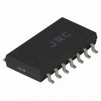
IC OPAMP J-FET QUAD 14-DMP
Manufacturer
NJR
Datasheet
1.NJM074M.pdf
(2 pages)
Specifications of NJM074M#
Amplifier Type
J-FET
Number Of Circuits
4
Slew Rate
13 V/µs
Gain Bandwidth Product
3MHz
Current - Input Bias
30pA
Voltage - Input Offset
3000µV
Current - Supply
6mA
Voltage - Supply, Single/dual (±)
±4 V ~ 18 V
Operating Temperature
-20°C ~ 75°C
Mounting Type
Surface Mount
Package / Case
14-DMP
Lead Free Status / RoHS Status
Lead free / RoHS Compliant
Output Type
-
Current - Output / Channel
-
-3db Bandwidth
-
Other names
NJM#074M
NJM#074M
NJM#074M
Available stocks
Company
Part Number
Manufacturer
Quantity
Price


■ GENERAL DESCRIPTION
NJM072B/082B except supply current.
■ FEATURES
■ PIN CONFIGURATION
■ EQUIVALENT CIRCUIT ( 1/4 Shown )
Ver.2003-03-17
● Operating Voltage
● J-FET Input
● High Input Resistance
● Low Input Bias Current
● High Slew Rate
● Wide Unity Gain Bandwidth ( 3MHz typ. )
● Package Outline
● Bipolar Technology
The NJM074/084 are quad JFET input operational amplifiers.
The NJM074/084 have the same electrical characteristics of
QUAD J-FET INPUT OPERATIONAL AMPLIFIER
( ±4V~±18V )
( 10
( 130pA typ. )
( 13V/µs typ. )
DIP14,DMP14,SSOP14
12
Ω
typ. )
NJM074D/084D
NJM074M/084M
NJM074V/084V
PIN FUNCTION
1. A OUTPUT
2. A -INPUT
3. A +INPUT
4. V
5. B +INPUT
6. B -INPUT
7. B OUTPUT
8. C OUTPUT
9. C –INPUT
10.C +INPUT
11.V
12.D +INPUT
13.D –INPUT
14.D OUTPUT
■ PACKAGE OUTLINE
+
-
NJM074D
NJM084D
NJM074V
NJM084V
NJM074M
NJM084M
- 1 -
Related parts for NJM074M#
Image
Part Number
Description
Manufacturer
Datasheet
Request
R

Part Number:
Description:
Quad J-FET Input Operational Amplifier
Manufacturer:
NJR Corporation
Datasheet:


Part Number:
Description:
Op Amps Single Full Swing Lead Free Package
Manufacturer:
NJR

Part Number:
Description:
Operational Amplifiers - Op Amps Dual Full Swing
Manufacturer:
NJR
Part Number:
Description:
Operational Amplifiers - Op Amps Dual High Gain Lead Free Package
Manufacturer:
NJR
Part Number:
Description:
Operational Amplifiers - Op Amps Dual High Gain
Manufacturer:
NJR
Part Number:
Description:
Operational Amplifiers - Op Amps Dual LwNoise PreAmp
Manufacturer:
NJR
NJM074M# Summary of contents
Page 1
QUAD J-FET INPUT OPERATIONAL AMPLIFIER ■ GENERAL DESCRIPTION The NJM074/084 are quad JFET input operational amplifiers. The NJM074/084 have the same electrical characteristics of NJM072B/082B except supply current. ■ FEATURES ● Operating Voltage ( ±4V~±18V ) ● J-FET Input ● ...
Page 2
ABSOLUTE MAXIMUM RATINGS PARAMETER Supply Voltage Differential Input Voltage Input Voltage Power Dissipation Operating Temperature Range Storage Temperature Range ( note1 ) For supply voltage less than ±15V. the absolute maximum input voltage is equal to the supply voltage. ...