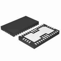
LT6604CUFF-5#PBF Linear Technology, LT6604CUFF-5#PBF Datasheet - Page 13

LT6604CUFF-5#PBF
Manufacturer Part Number
LT6604CUFF-5#PBF
Description
IC AMP DIFF LN DUAL 34-QFN
Manufacturer
Linear Technology
Specifications of LT6604CUFF-5#PBF
Amplifier Type
Differential
Number Of Circuits
2
Output Type
Differential
Current - Input Bias
30µA
Voltage - Input Offset
8000µV
Current - Supply
30mA
Voltage - Supply, Single/dual (±)
3 V ~ 11 V, ±1.5 V ~ 5.5 V
Operating Temperature
0°C ~ 70°C
Mounting Type
Surface Mount
Package / Case
34-QFN
No. Of Amplifiers
2
Input Offset Voltage
35mV
Bandwidth
5MHz
Supply Voltage Range
3V To 11V
Supply Current
30mA
Amplifier Case Style
QFN
No. Of Pins
34
Rohs Compliant
Yes
Lead Free Status / RoHS Status
Lead free / RoHS Compliant
Current - Output / Channel
-
-3db Bandwidth
-
Slew Rate
-
Gain Bandwidth Product
-
Available stocks
Company
Part Number
Manufacturer
Quantity
Price
APPLICATIONS INFORMATION
Junction temperature, T
temperature, T
dissipation is the product of supply voltage, V
supply current, I
given by:
where the supply current, I
load impedance, temperature and common mode volt-
ages. For a given supply voltage, the worst-case power
dissipation occurs when the differential input signal is
maximum, the common mode currents are maximum (see
the Applications Information section regarding Common
Mode DC Currents), the load impedance is small and
TYPICAL APPLICATIONS
T
J
= T
A
+ (P
(1V-1.5V)
Dual, Matched, 5MHz Lowpass Filter
V
D
A
OCM
Q
I
IN
, and power dissipation, P
IN
S
• θ
. Therefore, the junction temperature is
0.01μF
0.01μF
JA
R
R
R
R
) = T
IN
IN
IN
IN
J
, is calculated from the ambient
34
12
14
10
A
4
6
2
8
S
+ (V
, is a function of signal level,
–
–
+
+
1/2
LT6604-5
1/2
LT6604-5
3V
3V
25
7
17
24
+
+
–
–
S
0.1μF
0.1μF
• I
27
29
19
21
S
• θ
GAIN =
JA
Q
I
OUT
OUT
)
D
. The power
806Ω
S
R
IN
, and total
the ambient temperature is maximum. To compute the
junction temperature, measure the supply current under
these worst-case conditions, use 43°C/W as the package
thermal resistance, then apply the equation for T
example, using the circuit in Figure 3 with DC differential
input voltage of 250mV, a differential output voltage of 1V,
1k load resistance and an ambient temperature of 85°C,
the supply current (current into V
channel. The resulting junction temperature is: T
(P
resistance can be affected by the amount of copper on the
PCB that is connected to V
circuit can increase if the exposed pad is not connected
to a large ground plane with a number of vias.
D
• θ
JA
) = 85 + (5 • 2 • 0.0322 • 43) = 99°C. The thermal
30
25
20
15
10
5
0
–134.5 –134 –133.5 –133 –132.5 –132
5MHz Phase Distribution
5MHz PHASE (DEG)
(50 Units)
–
. The thermal resistance of the
+
) measures 32.2mA per
LT6604-5
66045 TA02
J
13
= T
J
. For
66045fa
A
+


