LT6604CUFF-15#PBF Linear Technology, LT6604CUFF-15#PBF Datasheet - Page 9
LT6604CUFF-15#PBF
Manufacturer Part Number
LT6604CUFF-15#PBF
Description
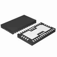
IC AMP DIFF LN DUAL 34-QFN
Manufacturer
Linear Technology
Datasheet
1.LT6604IUFF-15PBF.pdf
(16 pages)
Specifications of LT6604CUFF-15#PBF
Amplifier Type
Differential
Number Of Circuits
2
Output Type
Differential
Current - Input Bias
35µA
Voltage - Input Offset
10000µV
Current - Supply
38mA
Voltage - Supply, Single/dual (±)
3 V ~ 11 V, ±1.5 V ~ 5.5 V
Operating Temperature
0°C ~ 70°C
Mounting Type
Surface Mount
Package / Case
34-QFN
No. Of Amplifiers
2
Input Offset Voltage
35mV
Bandwidth
15MHz
Supply Voltage Range
3V To 11V
Supply Current
38mA
Amplifier Case Style
QFN
No. Of Pins
34
Rohs Compliant
Yes
Lead Free Status / RoHS Status
Lead free / RoHS Compliant
Current - Output / Channel
-
-3db Bandwidth
-
Slew Rate
-
Gain Bandwidth Product
-
Available stocks
Company
Part Number
Manufacturer
Quantity
Price


APPLICATIONS INFORMATION
Interfacing to the LT6604-15
Note: The LT6604-15 contains two identical fi lters. The
following applications information only refers to one fi lter.
The two fi lters are independent except that they share the
same negative supply voltage V
used simultaneously by replicating the example circuits.
The referenced pin numbers correspond to the A channel
fi lter
The LT6604-15 channel requires two equal external re-
sistors, R
inputs to the fi lter are the voltages V
to these external components, Figure 1. The difference
between V
average of V
Similarly, the voltages V
27 and 29 of the LT6604-15 are the fi lter outputs. The dif-
ference between V
voltage. The average of V
IN
IN
, to set the differential gain to 536Ω/R
IN
+
+
and V
–1
2
1
0
and V
3
2
1
0
V
OUT
V
IN
IN
–
+
–
is the differential input voltage. The
and V
is the common mode input voltage.
OUT
OUT
V
+
IN
V
V
OUT
and V
+
IN
+
IN
+
–
and V
–
–
. The two fi lters can be
is the differential output
OUT
IN
OUT
t
+
t
and V
–
appearing at Pins
V
–
V
V
IN
IN
IN
is the common
+
–
+
IN
0.1μF
0.1μF
536Ω
–
536Ω
presented
536Ω
536Ω
0.01μF
IN
. The
0.01μF
34
4
6
2
Figure 1
Figure 2
1/2
LT6604-15
–
+
25
34
3.3V
7
4
6
2
mode output voltage. Figure 1 illustrates the LT6604-15
operating with a single 3.3V supply and unity passband
gain; the input signal is DC coupled. The common mode
input voltage is 0.5V, and the differential input voltage is
2V
differential output voltage is 2V
15MHz. The common mode output voltage is determined
by the voltage at V
the output common mode is the mid-supply voltage. In
addition, the common mode input voltage can be equal
to the mid-supply voltage of V
Figure 2 shows how to AC couple signals into the LT6604-15.
In this instance, the input is a single-ended signal. AC cou-
pling allows the processing of single-ended or differential
signals with arbitrary common mode levels. The 0.1μF
coupling capacitor and the 536Ω gain setting resistor
form a high pass fi lter, attenuating signals below 3kHz.
Larger values of coupling capacitors will proportionally
reduce this highpass 3dB frequency.
1/2
LT6604-15
+
–
+
–
25
0.1μF
3.3V
27
7
29
P-P
+
–
0.1μF
27
. The common mode output voltage is 1.65V, and the
29
V
V
OUT
OUT
+
–
V
V
OUT
OUT
+
–
OCM
3
2
1
0
V
3
2
1
0
. Since V
V
MID
V
V
P-P
OUT
OUT
OCM
V
V
OUT
OUT
.
+
–
660415 F01
for frequencies below
+
–
660415 F02
LT6604-15
is shorted to V
t
660415fb
MID
9
,
Related parts for LT6604CUFF-15#PBF
Image
Part Number
Description
Manufacturer
Datasheet
Request
R

Part Number:
Description:
IC AMP DIFF LN DUAL 34-QFN
Manufacturer:
Linear Technology
Datasheet:
Part Number:
Description:
IC AMP DIFF LN DUAL 34-QFN
Manufacturer:
Linear Technology
Datasheet:
Part Number:
Description:
IC AMP DIFF LN DUAL 34-QFN
Manufacturer:
Linear Technology
Datasheet:
Part Number:
Description:
IC AMP DIFF LN DUAL 34-QFN
Manufacturer:
Linear Technology
Datasheet:
Part Number:
Description:
IC AMP DIFF LN DUAL 34-QFN
Manufacturer:
Linear Technology
Datasheet:
Part Number:
Description:
IC AMP DIFF LN DUAL 34-QFN
Manufacturer:
Linear Technology
Datasheet:
Part Number:
Description:
IC AMP DIFF LN DUAL 34-QFN
Manufacturer:
Linear Technology
Datasheet:

Part Number:
Description:
Dual Very Low Noise, Differential Amplifi er and 2.5MHz Lowpass Filter
Manufacturer:
LINER [Linear Technology]
Datasheet:
Part Number:
Description:
Dual Very Low Noise, Differential Amplifi er and 5MHz Lowpass Filter
Manufacturer:
LINER [Linear Technology]
Datasheet:

Part Number:
Description:
CD ROM LINEARVIEW DATASHEETS
Manufacturer:
Linear Technology

Part Number:
Description:
Standalone Linear Li-Ion Battery Charger with Thermal Regulation in ThinSOT
Manufacturer:
Linear Technology Corporation
Datasheet:
Part Number:
Description:
Low noise, high frequency, 8th order linear phase lowpass filter
Manufacturer:
Linear Technology Corporation
Datasheet:
Part Number:
Description:
Manufacturer:
Linear Technology Corporation
Datasheet:
Part Number:
Description:
Manufacturer:
Linear Technology Corporation
Datasheet:
Part Number:
Description:
Manufacturer:
Linear Technology Corporation
Datasheet: