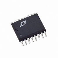
LT1362CS Linear Technology, LT1362CS Datasheet - Page 9

LT1362CS
Manufacturer Part Number
LT1362CS
Description
IC OP-AMP HISPD 50MHZ QUAD16SOIC
Manufacturer
Linear Technology
Series
C-Load™r
Datasheet
1.LT1361CS8PBF.pdf
(12 pages)
Specifications of LT1362CS
Amplifier Type
Voltage Feedback
Number Of Circuits
4
Slew Rate
800 V/µs
Gain Bandwidth Product
50MHz
Current - Input Bias
300nA
Voltage - Input Offset
300µV
Current - Supply
4mA
Current - Output / Channel
34mA
Voltage - Supply, Single/dual (±)
±2.5 V ~ 15 V
Operating Temperature
0°C ~ 70°C
Mounting Type
Surface Mount
Package / Case
16-SOIC (3.9mm Width)
Lead Free Status / RoHS Status
Contains lead / RoHS non-compliant
Output Type
-
-3db Bandwidth
-
Available stocks
Company
Part Number
Manufacturer
Quantity
Price
Company:
Part Number:
LT1362CS
Manufacturer:
LT
Quantity:
4 500
Part Number:
LT1362CS
Manufacturer:
LT/凌特
Quantity:
20 000
Company:
Part Number:
LT1362CS#PBF
Manufacturer:
Intersil
Quantity:
5 000
Part Number:
LT1362CS#PBF
Manufacturer:
LINEAR/凌特
Quantity:
20 000
Part Number:
LT1362CS#TRPBF
Manufacturer:
LINEAR/凌特
Quantity:
20 000
TYPICAL PERFORMANCE CHARACTERISTICS
Small-Signal Transient
(A
Large-Signal Transient
(A
Layout and Passive Components
The LT1361/LT1362 amplifiers are easy to use and toler-
ant of less than ideal layouts. For maximum performance
(for example, fast 0.01% settling) use a ground plane,
short lead lengths, and RF-quality bypass capacitors
(0.01 F to 0.1 F). For high drive current applications use
low ESR bypass capacitors (1 F to 10 F tantalum). The
parallel combination of the feedback resistor and gain
setting resistor on the inverting input combine with the
input capacitance to form a pole which can cause peaking
or oscillations. If feedback resistors greater than 5k are
used, a parallel capacitor of value
should be used to cancel the input pole and optimize
dynamic performance. For unity-gain applications where
a large feedback resistor is used, C
than or equal to C
APPLICATIONS
V
V
C
= 1)
= 1)
F
> R
G
x C
IN
/R
IN
F
U
.
1361/1362 TA31
1361/1362 TA34
INFORMATION
U
W
U
W
F
should be greater
Small-Signal Transient
(A
Large-Signal Transient
(A
V
V
= –1)
= –1)
U
Input Considerations
Each of the LT1361/LT1362 inputs is the base of an NPN
and a PNP transistor whose base currents are of opposite
polarity and provide first-order bias current cancellation.
Because of variation in the matching of NPN and PNP beta,
the polarity of the input bias current can be positive or
negative. The offset current does not depend on NPN/PNP
beta matching and is well controlled. The use of balanced
source resistance at each input is recommended for
applications where DC accuracy must be maximized.
The inputs can withstand transient differential input volt-
ages up to 10V without damage and need no clamping or
source resistance for protection. Differential inputs, how-
ever, generate large supply currents (tens of mA) as
required for high slew rates. If the device is used with
sustained differential inputs, the average supply current
will increase, excessive power dissipation will result and
the part may be damaged. The part should not be used as
a comparator, peak detector or other open-loop applica-
1361/1362 TA35
1361/1362 TA32
Large-Signal Transient
(A
Small-Signal Transient
(A
V
V
= 1, C
= –1, C
L
L
= 10,000pF)
= 500pF)
LT1361/LT1362
1361/1362 TA33
1361/1362 TA36
9


