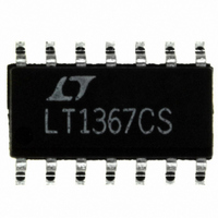
LT1367CS Linear Technology, LT1367CS Datasheet

LT1367CS
Specifications of LT1367CS
Available stocks
Related parts for LT1367CS
LT1367CS Summary of contents
Page 1
... Supply Current Sensing at Either Rail n Driving A/D Converters n L, LT, LTC, LTM, Over-The-Top, Linear Technology and the Linear logo are registered trademarks and C-Load is a trademark of Linear Technology Corporation. All other trademarks are the property of their respective owners. Typical applicaTion Positive Supply Rail Current Sense V ...
Page 2
... PLASTIC 150°C, θ = 150°C/W JMAX JA ORDER PART NUMBER PLASTIC (N) SURFACE MOUNT(S) LT1366CN8 LT1366CS8 LT1367CS LT1368CN8 LT1368CS8 LT1369CS SPECIFIED TEMPERATURE RANGE 0°C to 70°C 0°C to 70°C 0°C to 70°C 0°C to 70°C 0°C to 70°C 0°C to 70°C ...
Page 3
SYMBOL PARAMETER V Input Offset Voltage (LT1366/LT1368) OS Input Offset Voltage (LT1367/LT1369) Input Offset Voltage Shift (LT1366/LT1368) ∆V OS Input Offset Voltage Match (Channel to Channel) Input Offset Voltage Shift (LT1367/LT1369) Input Offset Voltage Match (Channel to Channel) ...
Page 4
LT1366/LT1367 LT1368/LT1369 elecTrical characTerisTics temperature range of 0°C < T < 70° SYMBOL PARAMETER V Input Offset Voltage (LT1366/LT1368) OS Input Offset Voltage (LT1367/LT1369 Input Offset Voltage Drift OS Input Offset Voltage Shift (LT1366/LT1368) ∆V OS ...
Page 5
SYMBOL PARAMETER Input Offset Current Shift ∆I OS Input Bias Current Match (Channel to Channel) A Large-Signal Voltage Gain VOL CMRR Common Mode Rejection Ratio (LT1366/LT1368) CMRR Match (Channel to Channel) Common Mode Rejection Ratio (LT1367/LT1369) CMRR Match ...
Page 6
LT1366/LT1367 LT1368/LT1369 elecTrical characTerisTics SYMBOL PARAMETER V Input Offset Voltage (LT1366/LT1368) OS Input Offset Voltage (LT1367/LT1369) ∆V Input Offset Voltage Shift (LT1366/LT1368) OS Input Offset Voltage Match (Channel to Channel) Input Offset Voltage Shift (LT1367/LT1369) Input Offset Voltage Match (Channel ...
Page 7
T < 70° SYMBOL PARAMETER V Input Offset Voltage (LT1366/LT1368) OS Input Offset Voltage (LT1367/LT1369) Input Offset Voltage Shift (LT1366/LT1368) ∆V OS Input Offset Voltage Match (Channel to Channel) Input Offset ...
Page 8
LT1366/LT1367 LT1368/LT1369 Typical perForMance characTerisTics (The data presented here applies to the LT1366/LT1367/LT1368/LT1369 unless otherwise noted.) PNP Stage V Distribution OS (LT1366/LT1368) 30 N-PACKAGE –350 ...
Page 9
Typical perForMance characTerisTics (The data presented here applies to the LT1366/LT1367/LT1368/LT1369 unless otherwise noted.) Minimum Supply Voltage 200 150 T = 70° 85°C A 100 25° –55°C A NONFUNCTIONAL 1 ...
Page 10
LT1366/LT1367 LT1368/LT1369 Typical perForMance characTerisTics (The data presented here applies to the LT1366/LT1367/LT1368/LT1369 unless otherwise noted.) Gain-Bandwidth and Phase Margin vs Supply Voltage (LT1366/LT1367) 500 450 GBW 400 PHASE MARGIN 350 300 250 200 150 100 ...
Page 11
Typical perForMance characTerisTics (The data presented here applies to the LT1366/LT1367/LT1368/LT1369 unless otherwise noted.) THD + Noise vs Frequency ±1. P 10k L 0 0.01 A ...
Page 12
LT1366/LT1367 LT1368/LT1369 applicaTions inForMaTion Technology’s proprietary complementary bipolar process, which ensures very similar DC and AC characteristics for the output devices Q24 and Q26. A simple comparator Q5 steers current from current source I between the two input stages. When ...
Page 13
Improved Supply Rejection in the LT1368/LT1369 The LT1368/LT1369 are variations of the LT1366/LT1367 offering greater supply rejection and lower high frequency output impedance. The LT1368/LT1369 require a 0.1µF load capacitance for compensation. The output capacitance forms a filter, ...
Page 14
LT1366/LT1367 LT1368/LT1369 Typical applicaTions Precision Low Dropout Regulator Microprocessors and complex digital circuits frequently specify tight control of power supply characteristics. The circuit shown in Figure 6 provides a precise 3.6V, 1A output from a minimum 3.8V input voltage. The ...
Page 15
Typical applicaTions High Side Current Source The wide compliance current source shown in Figure 7 takes advantage of the LT1366’s ability to measure small signals near the positive supply rail. The LT1366 adjusts Q1’s gate voltage to force the voltage ...
Page 16
LT1366/LT1367 LT1368/LT1369 Typical applicaTions the 2 op amp loop to create a negative summing junction 1 at A1’s positive input . The circuit has low sensitivities for center frequency and Q, which are set with the following equations: 2 ω ...
Page 17
DescripTion .300 – .325 (7.620 – 8.255) .065 (1.651) .008 – .015 TYP (0.203 – 0.381) +.035 .325 –.015 +0.889 8.255 –0.381 NOTE: INCHES 1. DIMENSIONS ARE MILLIMETERS *THESE DIMENSIONS DO NOT INCLUDE MOLD FLASH OR PROTRUSIONS. MOLD FLASH ...
Page 18
LT1366/LT1367 LT1368/LT1369 package DescripTion .050 BSC N .245 MIN .030 .005 TYP RECOMMENDED SOLDER PAD LAYOUT .010 – .020 45 (0.254 – 0.508) .008 – .010 (0.203 – 0.254) .016 – .050 (0.406 – 1.270) NOTE: INCHES ...
Page 19
... Updated Format of Order Information Section Change to Electrical Characteristics Note Information furnished by Linear Technology Corporation is believed to be accurate and reliable. However, no responsibility is assumed for its use. Linear Technology Corporation makes no representa- tion that the interconnection of its circuits as described herein will not infringe on existing patent rights. LT1366/LT1367 ...
Page 20
... LT1367 OUTPUT A1C – 100k 1366 TA03 OS(MAX) , 100nV/°C Drift, 1MHz GBW, OS(MAX) OS(MAX) and OS(MAX) , 2µV/°C Drift (Max), Over-The-Top ® Input LT 0310 REV B • PRINTED IN USA LINEAR TECHNOLOGY CORPORATION 1995 and and 1366fb ...


