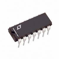
LT1125CN Linear Technology, LT1125CN Datasheet

LT1125CN
Specifications of LT1125CN
Available stocks
Related parts for LT1125CN
LT1125CN Summary of contents
Page 1
... LT1126/LT1127 data sheet. L, LT, LTC, LTM, Linear Technology and the Linear logo are registered trademarks of Linear Technology Corporation. All other trademarks are the property of their respective owners. Protected by U.S. Patents including 4775884, 4837496. ...
Page 2
LT1124/LT1125 ABSOLUTE MAXIMUM RATINGS (Note 1) Supply Voltage ........................................................±22V Input Voltages ............................Equal to Supply Voltage Output Short-Circuit Duration .......................... Indefi nite Differential Input Current (Note 6) .......................±25mA Lead Temperature (Soldering, 10 sec) .................. 300°C Storage Temperature Range ................... –65°C to ...
Page 3
... Plastic SO, Standard Pinout –55°C to 125°C LT1125CSW 16-Lead Plastic SO Wide LT1125MPSW 16-Lead Plastic SO Wide LT1124ACN8 8-Lead PDIP LT1124CN8 8-Lead PDIP LT1125ACN 14-Lead PDIP LT1125CN 14-Lead PDIP PART MARKING* PACKAGE DESCRIPTION 1124 8-Lead Plastic SO, Rotated Pinout 1124AI 8-Lead Plastic SO, Rotated Pinout 1124I 8-Lead Plastic SO, Rotated Pinout LT1125CSW ...
Page 4
LT1124/LT1125 ELECTRICAL CHARACTERISTICS SYMBOL PARAMETER V Input Offset Voltage OS ΔV Long-Term Input Offset OS ΔTime Voltage Stability I Input Offset Current OS I Input Bias Current B e Input Noise Voltage n Input Noise Voltage Density i Input Noise ...
Page 5
ELECTRICAL CHARACTERISTICS temperature range ±15V, unless otherwise noted. S SYMBOL PARAMETER V Input Offset Voltage OS ΔV Average Input Offset OS ΔTemp Voltage Drift I Input Offset Current OS I Input Bias Current B V Input Voltage Range ...
Page 6
LT1124/LT1125 ELECTRICAL CHARACTERISTICS Note 1: Stresses beyond those listed under Absolute Maximum Ratings may cause permanent damage to the device. Exposure to any Absolute Maximum Rating condition for extended periods may affect device reliability and lifetime. Note 2: Typical parameters ...
Page 7
TYPICAL PERFORMANCE CHARACTERISTICS Output Short-Circuit Current vs Time ±15V S 40 25°C 30 –55°C 20 125° –10 125°C –20 25°C –30 –55°C –40 – TIME FROM OUTPUT SHORT TO GND (MINUTES) ...
Page 8
LT1124/LT1125 TYPICAL PERFORMANCE CHARACTERISTICS Offset Voltage Drift with Temperature of Representative Units ±15V –10 –20 –30 –40 –50 –50 – 100 TEMPERATURE (°C) 1124/25 G14 Large-Signal Transient ...
Page 9
TYPICAL PERFORMANCE CHARACTERISTICS Total Harmonic Distortion and Noise vs Frequency for Noninverting Gain 0 2k/15pF 20V P +1, +10, +100 V MEASUREMENT BANDWIDTH = 10Hz TO 80kHz 0.010 A = +100 V ...
Page 10
LT1124/LT1125 APPLICATIONS INFORMATION The LT1124 may be inserted directly into OP-270 sock- ets. The LT1125 plugs into OP-470 sockets. Of course, all standard dual and quad bipolar op amps can also be replaced by these devices. Matching Specifi cations In ...
Page 11
APPLICATIONS INFORMATION High Speed Operation When the feedback around the op amp is resistive (R a pole will be created with R , the source resistance and F capacitance ( and the amplifi er input capacitance S ...
Page 12
... The comparison shows how the specs of the LT1124/ LT1125 not only stand up to the industry standard OP-27, Table 2. Guaranteed Performance ±15V LT1124CN8 PARAMETER/UNITS LT1125CN Voltage Noise, 1kHz 100% Tested Slew Rate 100% Tested Gain-Bandwidth Product 100% Tested Offset Voltage LT1124 ...
Page 13
SCHEMATIC DIAGRAM Q7 Q9 Q13 Q8 Q10 – V NONINVERTING INPUT (+) Q1A Q3 INVERTING INPUT (–) PACKAGE DESCRIPTION CORNER LEADS OPTION .045 – .068 (1.143 – 1.650) FULL LEAD OPTION .300 BSC (7.62 BSC) .008 – .018 (0.203 – ...
Page 14
LT1124/LT1125 PACKAGE DESCRIPTION .300 – .325 (7.620 – 8.255) .065 (1.651) TYP .008 – .015 (0.203 – 0.381) +.035 .325 –.015 +0.889 8.255 –0.381 NOTE: INCHES 1. DIMENSIONS ARE MILLIMETERS *THESE DIMENSIONS DO NOT INCLUDE MOLD FLASH OR PROTRUSIONS. MOLD ...
Page 15
PACKAGE DESCRIPTION .300 BSC (7.62 BSC) .008 – .018 (0.203 – 0.457) NOTE: LEAD DIMENSIONS APPLY TO SOLDER DIP/PLATE OR TIN PLATE LEADS .300 – .325 (7.620 – 8.255) .008 – .015 (0.203 – 0.381) +.035 .325 –.015 ( ) ...
Page 16
LT1124/LT1125 PACKAGE DESCRIPTION .030 ±.005 TYP N .420 MIN RECOMMENDED SOLDER PAD LAYOUT .291 – .299 (7.391 – 7.595) NOTE 4 .010 – .029 × 45° (0.254 – 0.737) .005 (0.127) RAD MIN .009 – .013 NOTE ...
Page 17
... Revised part marking for LT1124AMPS8-1 in Order Information section Information furnished by Linear Technology Corporation is believed to be accurate and reliable. However, no responsibility is assumed for its use. Linear Technology Corporation makes no representa- tion that the interconnection of its circuits as described herein will not infringe on existing patent rights. ...
Page 18
... Voltage Noise, 10fA/√Hz Current Noise 6nV/√Hz Voltage Noise, 1fA/√Hz Current Noise, 10pA Max I www.linear.com ● 10V OUTPUT 13 1μF 301k* 50k 499Ω* GAIN TRIM 1124/25 TA05 1010 REV E • PRINTED IN USA © LINEAR TECHNOLOGY CORPORATION 1992 11245fe ...


