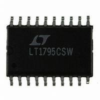
LT1795CSW Linear Technology, LT1795CSW Datasheet - Page 10

LT1795CSW
Manufacturer Part Number
LT1795CSW
Description
IC CRRNT FEEDBCK AMP DUAL 20SOIC
Manufacturer
Linear Technology
Datasheet
1.LT1795CSW.pdf
(12 pages)
Specifications of LT1795CSW
Amplifier Type
Current Feedback
Number Of Circuits
2
Slew Rate
900 V/µs
-3db Bandwidth
65MHz
Current - Input Bias
10µA
Voltage - Input Offset
3000µV
Current - Supply
29mA
Current - Output / Channel
1A
Voltage - Supply, Single/dual (±)
±5 V ~ 15 V
Operating Temperature
0°C ~ 70°C
Mounting Type
Surface Mount
Package / Case
20-SOIC (7.5mm Width)
Lead Free Status / RoHS Status
Contains lead / RoHS non-compliant
Output Type
-
Gain Bandwidth Product
-
Available stocks
Company
Part Number
Manufacturer
Quantity
Price
Part Number:
LT1795CSW
Manufacturer:
LINEAR/凌特
Quantity:
20 000
Part Number:
LT1795CSW#PBF
Manufacturer:
LINEAR/凌特
Quantity:
20 000
Company:
Part Number:
LT1795CSW#TR
Manufacturer:
LinearTec
Quantity:
17 236
Part Number:
LT1795CSW#TR
Manufacturer:
LT/凌特
Quantity:
20 000
Part Number:
LT1795CSW#TRPBF
Manufacturer:
LINEAR/凌特
Quantity:
20 000
Part Number:
LT1795CSWE
Manufacturer:
LT/凌特
Quantity:
20 000
APPLICATIONS
LT1795
PACKAGE DESCRIPTIO
10
Figure 9 shows the effect of the network on a 200pF load.
Without the optional compensation, there is a 6dB peak at
85MHz caused by the effect of the capacitance on the
output stage. Adding a 0.01 F bypass capacitor between
the output and the COMP pins connects the compensation
14
12
10
–2
–4
–6
8
6
4
2
0
1
V
C
S
L
= 15V
= 200pF
R
COMPENSATION
F
U
.030 .005
NOTE:
1. DIMENSIONS IN
2. DRAWING NOT TO SCALE
3. PIN 1 IDENT, NOTCH ON TOP AND CAVITIES ON THE BOTTOM OF PACKAGES ARE THE MANUFACTURING OPTIONS.
4. THESE DIMENSIONS DO NOT INCLUDE MOLD FLASH OR PROTRUSIONS.
= 1k
RAD MIN
(0.229 – 0.330)
(0.127)
.009 – .013
THE PART MAY BE SUPPLIED WITH OR WITHOUT ANY OF THE OPTIONS
MOLD FLASH OR PROTRUSIONS SHALL NOT EXCEED .006" (0.15mm)
.005
TYP
.420
MIN
FREQUENCY (MHz)
INFORMATION
Figure 9
U
RECOMMENDED SOLDER PAD LAYOUT
N
1
10
(MILLIMETERS)
(0.254 – 0.737)
2
INCHES
.010 – .029
NOTE 3
COMPENSATION
R
COMPENSATION
(7.391 – 7.595)
F
.291 – .299
= 3.4k
NOTE 4
W
R
3
(0.406 – 1.270)
F
.016 – .050
= 3.4k
NO
U
20-Lead Plastic Small Outline (Wide .300 Inch)
45
1795 F09
.050 BSC
100
N/2
(Reference LTC DWG # 05-08-1620)
U
.325 .005
.045 .005
0 – 8 TYP
NOTE 3
SW Package
(2.362 – 2.642)
.093 – .104
(1.270)
.050
BSC
and greatly reduces the peaking. A lower value feedback
resistor can now be used, resulting in a response which is
flat to 1dB to 45MHz. The network has the greatest effect
for C
Although the optional compensation works well with
capacitive loads, it simply reduces the bandwidth when it
is connected with resistive loads. For instance, with a 25
load, the bandwidth drops from 48MHz to 32MHz when
the compensation is connected. Hence, the compensation
was made optional. To disconnect the optional compensa-
tion, leave the COMP pin open.
DEMO BOARD
A demo board (DC261A) is available for evaluating the
performence of the LT1795. The board is configured as a
differential line driver/receiver suitable for xDSL applica-
tions. For details, consult your local sales representative.
20
N
1
(0.356 – 0.482)
.014 – .019
19
2
TYP
L
18
3
in the range of 0pF to 1000pF.
17
(12.598 – 13.005)
4
.496 – .512
16
NOTE 4
5
15
6
14
7
13
8
12
9
N/2
11
10
(0.940 – 1.143)
.037 – .045
(0.102 – 0.305)
(10.007 – 10.643)
.004 – .012
.394 – .419
S20 (WIDE) 0502
1795fa


