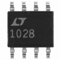
LT1028CS8 Linear Technology, LT1028CS8 Datasheet - Page 4

LT1028CS8
Manufacturer Part Number
LT1028CS8
Description
IC OP-AMP LOW NOISE SNGL 8-SOIC
Manufacturer
Linear Technology
Datasheet
1.LT1028CS8PBF.pdf
(20 pages)
Specifications of LT1028CS8
Amplifier Type
General Purpose
Number Of Circuits
1
Slew Rate
15 V/µs
Gain Bandwidth Product
75MHz
Current - Input Bias
30nA
Voltage - Input Offset
20µV
Current - Supply
7.6mA
Voltage - Supply, Single/dual (±)
±4 V ~ 18 V
Operating Temperature
-40°C ~ 85°C
Mounting Type
Surface Mount
Package / Case
8-SOIC (3.9mm Width)
Lead Free Status / RoHS Status
Contains lead / RoHS non-compliant
Output Type
-
Current - Output / Channel
-
-3db Bandwidth
-
Available stocks
Company
Part Number
Manufacturer
Quantity
Price
Company:
Part Number:
LT1028CS8#PBF
Manufacturer:
Linear Technology
Quantity:
1 913
Company:
Part Number:
LT1028CS8#PBF
Manufacturer:
Maxim
Quantity:
290
Part Number:
LT1028CS8#PBF
Manufacturer:
LINEAR/凌特
Quantity:
20 000
Company:
Part Number:
LT1028CS8#TRPBF
Manufacturer:
PANASONIC
Quantity:
560 000
Note 1: Absolute Maximum Ratings are those values beyond which the life
of a device may be impaired.
Note 2: Input Offset Voltage measurements are performed by automatic
test equipment approximately 0.5 sec. after application of power. In
addition, at T
approximately 55 C to account for the chip temperature rise when the
device is fully warmed up.
Note 3: Long Term Input Offset Voltage Stability refers to the average
trend line of Offset Voltage vs. Time over extended periods after the first
30 days of operation. Excluding the initial hour of operation, changes in
V
Note 4: This parameter is tested on a sample basis only.
Note 5: 10Hz noise voltage density is sample tested on every lot with the
exception of the S8 and S16 packages. Devices 100% tested at 10Hz are
available on request.
Note 6: Current noise is defined and measured with balanced source
resistors. The resultant voltage noise (after subtracting the resistor noise
SYMBOL PARAMETER
V
I
I
CMRR
PSRR
A
V
I
SYMBOL PARAMETER
V
I
I
CMRR
PSRR
A
V
I
LT1028/LT1128
ELECTRICAL C
0 C T
ELECTRICAL C
4
OS
B
S
– 40 C T
OS
B
S
OS
OS
VOL
OUT
OS
VOL
OUT
Temp
Temp
V
V
OS
OS
during the first 30 days are typically 2.5 V.
A
Input Offset Voltage
Average Input Offset Drift
Input Offset Current
Input Bias Current
Input Voltage Range
Common Mode Rejection Ratio
Power Supply Rejection Ratio
Large-Signal Voltage Gain
Maximum Output Voltage Swing
Supply Current
Input Offset Voltage
Average Input Offset Drift
Input Offset Current
Input Bias Current
Input Voltage Range
Common Mode Rejection Ratio
Power Supply Rejection Ratio
Large-Signal Voltage Gain
Maximum Output Voltage Swing
Supply Current
A
70 C. V
A
= 25 C, offset voltage is measured with the chip heated to
85 C. V
S
= 15V, unless otherwise noted.
S
= 15V, unless otherwise noted. (Note 11)
HARA TERISTICS
HARA TERISTICS
C
C
(Note 8)
R
CONDITIONS
(Note 2)
(Note 8)
V
V
V
V
R
R
R
R
CONDITIONS
V
V
V
V
R
R
CM
CM
CM
S
CM
CM
CM
S
L
L
L
L
L
L
L
= 4.5V to 18V
= 4.5V to 18V
= 0V
= 0V
= 10.5V
= 0V
= 0V
= 10.5V
2k, V
1k, V
2k
600 (Note 10)
2k, V
1k, V
2k
O
O
O
O
= 10V
= 10V
= 10V
= 10V
The
The
denotes the specifications which apply over the temperature range
denotes the specifications which apply over the temperature range
on an RMS basis) is divided by the sum of the two source resistors to
obtain current noise. Maximum 10Hz current noise can be inferred from
100% testing at 1kHz.
Note 7: Gain-bandwidth product is not tested. It is guaranteed by design
and by inference from the slew rate measurement.
Note 8: This parameter is not 100% tested.
Note 9: The inputs are protected by back-to-back diodes. Current-limiting
resistors are not used in order to achieve low noise. If differential input
voltage exceeds 1.8V, the input current should be limited to 25mA.
Note 10: This parameter guaranteed by design, fully warmed up at T
70 C. It includes chip temperature increase due to supply and load
currents.
Note 11: The LT1028/LT1128 are designed, characterized and expected to
meet these extended temperature limits, but are not tested at –40 C and
85 C. Guaranteed I grade parts are available. Consult factory.
MIN
MIN
110
114
108
112
10.5
5.0
4.0
11.5
10.4
4.0
3.0
11.0
9.5
LT1028AC
LT1128AC
LT1028AC
LT1128AC
25.0
18.0
20.0
14.0
TYP
TYP
124
132
123
131
0.1
12.0
12.7
11.0
8.0
0.2
11.8
12.5
8.5
20
20
15
15
30
35
MAX
MAX
10.5
11.0
0.8
0.8
80
65
95
80
140
120
MIN
MIN
102
106
106
107
10.5
3.0
2.5
11.5
10.4
2.5
2.0
11.0
9.0
LT1028C
LT1128C
LT1028C
LT1128C
25.0
18.0
0.25
20.0
14.0
TYP
TYP
124
132
123
131
0.2
12.0
12.7
10.5
8.2
11.8
12.5
8.7
35
28
30
22
45
40
MAX
MAX
11.5
12.5
150
160
125
130
1.0
1.0
280
240
UNITS
UNITS
A
V/ V
V/ V
V/ C
V/ V
V/ V
=
V/ C
mA
mA
nA
nA
dB
dB
nA
nA
dB
dB
V
V
V
V
V
V
V


