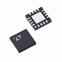
LTC6404IUD-1#TRPBF Linear Technology, LTC6404IUD-1#TRPBF Datasheet - Page 25

LTC6404IUD-1#TRPBF
Manufacturer Part Number
LTC6404IUD-1#TRPBF
Description
IC AMP/DRIVER DIFF 16-QFN
Manufacturer
Linear Technology
Type
ADC Driverr
Datasheet
1.LTC6404CUD-1PBF.pdf
(28 pages)
Specifications of LTC6404IUD-1#TRPBF
Applications
Data Acquisition
Mounting Type
Surface Mount
Package / Case
16-WQFN Exposed Pad
Current - Supply
27.8mA
Operating Temperature
-40°C ~ 85°C
Output Type
Differential, Rail-to-Rail
Number Of Circuits
1
Current - Output / Channel
85mA
Amplifier Type
Differential
Voltage - Supply, Single/dual (±)
2.7 V ~ 5.5 V, ±1.35 V ~ 2.75 V
-3db Bandwidth
600MHz
Slew Rate
450 V/µs
Gain Bandwidth Product
500MHz
Current - Input Bias
23µA
Voltage - Input Offset
500µV
Lead Free Status / RoHS Status
Lead free / RoHS Compliant
Available stocks
Company
Part Number
Manufacturer
Quantity
Price
APPLICATIONS INFORMATION
The LTC6404’s input referred voltage noise contributes the
equivalent noise of a 140Ω resistor. When the feedback
network is comprised of resistors whose values are less
than this, the LTC6404’s output noise is voltage noise
dominant (See Figure 10.):
Feedback networks consisting of resistors with values
greater than about 200Ω will result in output noise which
is resistor noise and amplifi er current noise dominant.
Lower resistor values (<100Ω) always result in lower noise
at the penalty of increased distortion due to increased load-
ing of the feedback network on the output. Higher resistor
values (but still less than 400Ω) will result in higher output
noise, but improved distortion due to less loading on the
output. The optimal feedback resistance for the LTC6404
runs between 100Ω to 400Ω. Higher resistances are not
recommended.
The differential fi ltered outputs OUTF
a little higher spot noise than the unfi ltered outputs (due to
the two 50Ω resistors which contribute 0.9nV/√Hz each),
but actually will provide superior Signal-to-Noise in noise
bandwidths exceeding 139MHz due to the noise-fi ltering
function the fi lter provides.
e
e
no
no
Figure 10. LTC6404-1 Output Spot Noise vs Spot Noise
Contributed by Feedback Network Alone
≈
≈
e
100
0.1
ni
10
2
1
• 1
10
•
⎛
⎝ ⎜
+
(
TOTAL (AMPLIFIER AND
I R
n
FEEDBACK NETWORK)
R
R
•
F
I
⎞
⎠ ⎟
100
F
OUTPUT NOISE
)
R
2
FEEDBACK RESISTOR
NETWORK NOISE ALONE
F
= R
+
⎛
⎝ ⎜
I
(Ω)
1
+
1k
R
R
F
I
⎞
⎠ ⎟
+
and OUTF
• • • •
4
6404 F10
10k
k T R
–
will have
F
Layout Considerations
Because the LTC6404 is a very high speed amplifi er, it is
sensitive to both stray capacitance and stray inductance.
Three pairs of power supply pins are provided to keep the
power supply inductance as low as possible to prevent
degradation of amplifi er 2nd Harmonic performance. It is
critical that close attention be paid to supply bypassing. For
single supply applications (Pins 3, 9 and 12 grounded) it
is recommended that 3 high quality 0.1μF surface mount
ceramic bypass capacitor be placed between pins 2 and
3, between pins 11and 12, and between pins10 and 9 with
direct short connections. Pins 3, 9 and 10 should be tied
directly to a low impedance ground plane with minimal
routing. For dual (split) power supplies, it is recommended
that at least two additional high quality, 0.1μF ceramic
capacitors are used to bypass pin V
ground, again with minimal routing. For driving large loads
(<200Ω), additional bypass capacitance may be needed for
optimal performance. Keep in mind that small geometry
(e.g. 0603) surface mount ceramic capacitors have a much
higher self resonant frequency than do leaded capacitors,
and perform best in high speed applications.
Any stray parasitic capacitances to ground at the sum-
ming junctions IN
minimum even if it means stripping back the ground plane
away from any trace attached to this node. This becomes
especially true when the feedback resistor network uses
resistor values >400Ω in circuits with R
peaking in the frequency response can be mitigated by add-
ing small amounts of feedback capacitance (0.5pF to 2pF)
around R
the LTC6404, and that it is critical that the load impedances
seen by both outputs (stray or intended) should be as bal-
anced and symmetric as possible. This will help preserve
the natural balance of the LTC6404, which minimizes the
generation of even order harmonics, and preserves the
rejection of common mode signals and noise.
It is highly recommended that the V
tied to a low impedance ground plane (in split supply
applications), or bypassed to ground with a high quality
ceramic capacitor whose value exceeds 0.01μF . This will
help stabilize the common mode feedback loop as well as
prevent thermal noise from the internal voltage divider and
F
. Always keep in mind the differential nature of
+
, and IN
–
should be kept to an absolute
OCM
+
to ground and V
LTC6404
pin be either hard
F
= R
I
. Excessive
25
–
6404f
to


