TC7652IJA Microchip Technology, TC7652IJA Datasheet - Page 3
TC7652IJA
Manufacturer Part Number
TC7652IJA
Description
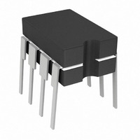
IC OPAMP CHOPPER STAB LN 8CDIP
Manufacturer
Microchip Technology
Datasheet
1.TC7652IJA.pdf
(16 pages)
Specifications of TC7652IJA
Amplifier Type
Chopper (Zero-Drift)
Number Of Circuits
1
Slew Rate
1 V/µs
Gain Bandwidth Product
400kHz
Current - Input Bias
30pA
Voltage - Input Offset
2000µV
Current - Supply
1mA
Voltage - Supply, Single/dual (±)
5 V ~ 16 V, ±2.5 V ~ 8 V
Operating Temperature
-25°C ~ 85°C
Mounting Type
Through Hole
Package / Case
8-CDIP (0.300", 7.62mm)
Lead Free Status / RoHS Status
Lead free / RoHS Compliant
Output Type
-
Current - Output / Channel
-
-3db Bandwidth
-


1.0
ABSOLUTE MAXIMUM RATINGS*
Total Supply Voltage (V
Input Voltage .................... (V
Voltage on Oscillator Control Pins...............V
Duration of Output Short Circuit ..................... Indefinite
Current Into Any Pin............................................ 10mA
Package Power Dissipation (T
Storage Temperature Range .............. -65°C to +150°C
Operating Temperature Range
TC7652 ELECTRICAL SPECIFICATIONS
©
Electrical Characteristics: V
V
TCV
V
I
I
I
R
OL
V
CMVR
MRR
PSRR
e
I
GBW
SR
V
Note 1: Limiting input current to 100µA is recommended to avoid latch-up problems. Typically 1mA is safe however, this is not
BIAS
BIAS
OS
N
N
OS
OS
OUT
DD
2002 Microchip Technology Inc.
IN
Symbol
/DT
, V
While Operating (Note 1)............................ 100µA
8-Pin Plastic DIP ....................................... 730mW
14-Pin Plastic DIP ..................................... 800mW
C Device .......................................... 0°C to +70°C
I Device ......................................... -25°C to +85°C
OS
SS
2: Output clamp not connected. See typical characteristics curves for output swing versus clamp current characteristics.
3: See “Output Clamp” under detailed description.
ELECTRICAL
CHARACTERISTICS
guaranteed.
Input Offset Voltage
Average Temperature Co-efficient of
Input Offset Voltage
Offset Voltage vs Time
Input Bias Current (CLK On)
Input Bias Current (CLK Off)
Input Offset Current
Input Resistance
Large Signal Voltage Gain
Output Voltage Swing (Note 2)
Common Mode Voltage Range
Common Mode Rejection Ratio
Power Supply
Input Noise Voltage
Input Noise Current
Unity Gain Bandwidth
Slew Rate
Overshoot
Operating Supply Range
DD
Parameter
to V
DD
DD
A
= +5V, V
SS
+0.3V) to (V
< 70°C)
) .......................+18V
SS
= -5V, T
SS
DD
– 0.3V)
A
to V
= +25°C, unless otherwise indicated.
±4.7
Min
-4.3
120
120
120
SS
—
—
—
—
—
—
—
—
—
—
—
—
—
—
—
—
—
—
5
±4.85
±4.95
0.01
10
0.01
Typ
150
100
250
100
150
140
140
0.2
0.7
0.4
±2
30
15
35
25
15
*Stresses above those listed under “Absolute Maximum
Ratings” may cause permanent damage to the device.
These are stress ratings only and functional operation of the
device at these or any other conditions above those indi-
cated in the operation sections of the specifications is not
implied. Exposure to Absolute Maximum Rating conditions
for extended periods my affect device reliability.
—
—
1
12
1000
1000
Max
0.05
+3.5
100
150
1.5
±5
30
16
—
—
—
—
—
—
—
—
—
—
—
—
—
5
V/µsec C
nV/mo
µV/°C 0°C < T
Units
µV
µV
MHz
√Hz
pA/
µV
pA
pA
pA
dB
dB
dB
Ω
%
V
V
V
P-P
P-P
T
T
0°C < T
-25°C < T
T
0°C < T
-25°C < T
R
R
R
CMVR = -4.3V to +3.5V
±3V to ±8V
R
DC to 10Hz
f = 10Hz
A
A
A
L
L
L
S
L
= +25°C
= +25°C
= +25°C
= 10kΩ, V
= 10kΩ
= 100kΩ
= 50pF, R
= 100Ω, DC to 1Hz
Test Conditions
A
A
A
TC7652
< +70°C
< +70°C
< +70°C
A
A
< +85°C
< +85°C
DS21464B-page 3
L
OUT
= 10kΩ
= ±4V
Related parts for TC7652IJA
Image
Part Number
Description
Manufacturer
Datasheet
Request
R

Part Number:
Description:
Low Noise, Chopper Stabilized Operational Amplifier
Manufacturer:
Microchip Technology Inc.
Datasheet:
Part Number:
Description:
Manufacturer:
Microchip Technology Inc.
Datasheet:
Part Number:
Description:
Manufacturer:
Microchip Technology Inc.
Datasheet:
Part Number:
Description:
Manufacturer:
Microchip Technology Inc.
Datasheet:
Part Number:
Description:
Manufacturer:
Microchip Technology Inc.
Datasheet:
Part Number:
Description:
Manufacturer:
Microchip Technology Inc.
Datasheet:
Part Number:
Description:
Manufacturer:
Microchip Technology Inc.
Datasheet:
Part Number:
Description:
Manufacturer:
Microchip Technology Inc.
Datasheet:
Part Number:
Description:
Manufacturer:
Microchip Technology Inc.
Datasheet: