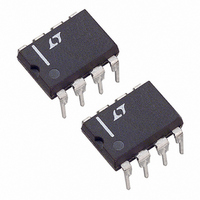
LTC1051CN8 Linear Technology, LTC1051CN8 Datasheet - Page 8

LTC1051CN8
Manufacturer Part Number
LTC1051CN8
Description
IC OPAMP CHOPR-STBL DUAL 8-DIP
Manufacturer
Linear Technology
Datasheet
1.LTC1051CN8PBF.pdf
(16 pages)
Specifications of LTC1051CN8
Amplifier Type
Chopper (Zero-Drift)
Number Of Circuits
2
Slew Rate
4 V/µs
Gain Bandwidth Product
2.5MHz
Current - Input Bias
15pA
Voltage - Input Offset
0.5µV
Current - Supply
1mA
Voltage - Supply, Single/dual (±)
4.75 V ~ 16 V, ±2.38 V ~ 8 V
Operating Temperature
0°C ~ 70°C
Mounting Type
Through Hole
Package / Case
8-DIP (0.300", 7.62mm)
Lead Free Status / RoHS Status
Contains lead / RoHS non-compliant
Output Type
-
Current - Output / Channel
-
-3db Bandwidth
-
Available stocks
Company
Part Number
Manufacturer
Quantity
Price
Company:
Part Number:
LTC1051CN8
Manufacturer:
LT
Quantity:
5 630
Part Number:
LTC1051CN8#PBF
Manufacturer:
LT/凌特
Quantity:
20 000
APPLICATIO S I FOR ATIO
LTC1051/LTC1053 as AC Amplifiers
Although initially chopper stabilized op amps were de-
signed to minimize DC offsets and offset drifts, the
LTC1051/LTC1053 family, on top of its outstanding DC
characteristics, presents efficient AC performance. For
instance, at single 5V supply, each op amp typically
consumes 0.5mA and still provides 1.8MHz gain band-
width product and 3V/µs slew rate. This, combined with
almost distortionless swing to the supply rails (Figure 8),
makes the LTC1051/LTC1053 op amps nearly general
purpose. To further expand this idea (the “aliasing” phe-
nomenon) which can occur under AC conditions, should
be described and properly evaluated.
LTC1051/LTC1053
8
20dBV
15dB
–100
/DIV
Figure 5a. Output Voltage Spectrum of 1/2 LTC1051 Operating as an Inverting Amplifier with Gain of 10,
and Amplifying a 750Hz/800mV, Input AC Signal
B: MAG
RANGE: 9dBV
START: 100Hz
X: 1825Hz
f
IN
U
= 750Hz
U
Figure 5b. Same as Figure 5a, but the AC Input Signal is 900mV, 10kHz
f
CLK
20dBV
15dB
–100
/DIV
– f
IN
W
BW: 47.742Hz
Y: – 70.72dBV
6f
A: MAG
RANGE: 11dBV
CENTER: 10 000Hz
X: 5550Hz
CLK
– f
IN
2f
U
IN
STATUS: PAUSED
2f
CLK
STOP: 5 100Hz
BW: 95.485Hz
Y: – 63.91dBV
f
IN
– f
= 10kHz
RMS: 25
IN
Aliasing
The LTC1051/LTC1053 are equipped with internal cir-
cuitry to minimize aliasing. Aliasing, no matter how small,
occurs when the input signal approaches and exceeds the
internal sampling rate. Aliasing is caused by the sampled
data nature of the chopper op amps. A generalized study
of this phenomenon is beyond the scope of a data sheet;
however, a set of rules of thumb can answer many
questions:
1. Alias signals can be generally defined as output AC
signals at a frequency of nf
internal sampling frequency of the chopper stabilized op
amps and its harmonics; mf
signal and its harmonics, if any.
80dB
STATUS: PAUSED
SPAN: 10 000Hz
f
0.8V
IN
R1
1k
P-P
RMS: 25
74dB
2
3
CLK
–
+
LTC1051
IN
1/2
– 5V
5V
± mf
is the frequency of the input
10k
R2
IN
. The nf
0.1µF
0.1µF
1
1051/53 F05a
50pF
CLK
V
OUT
term is the
10513fa


