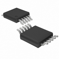
LT1969CMS#TR Linear Technology, LT1969CMS#TR Datasheet - Page 12

LT1969CMS#TR
Manufacturer Part Number
LT1969CMS#TR
Description
IC OP-AMP ADJ CURRNT DUAL 10MSOP
Manufacturer
Linear Technology
Datasheet
1.LT1969CMS.pdf
(20 pages)
Specifications of LT1969CMS#TR
Amplifier Type
General Purpose
Number Of Circuits
2
Slew Rate
200 V/µs
Gain Bandwidth Product
700MHz
Current - Input Bias
1.5µA
Voltage - Input Offset
1000µV
Current - Supply
7mA
Current - Output / Channel
700mA
Voltage - Supply, Single/dual (±)
4 V ~ 13 V, ±2 V ~ 6.5 V
Operating Temperature
0°C ~ 70°C
Mounting Type
Surface Mount
Package / Case
10-MSOP, Micro10™, 10-uMAX, 10-uSOP
Power Supply Requirement
Dual
Package Type
MSOP
Lead Free Status / RoHS Status
Contains lead / RoHS non-compliant
Output Type
-
-3db Bandwidth
-
Lead Free Status / Rohs Status
Not Compliant
Other names
LT1969CMSTR
Available stocks
Company
Part Number
Manufacturer
Quantity
Price
APPLICATIO S I FOR ATIO
LT1969
Capacitive Loading
The LT1969 is stable with a 1000pF capacitive load. The
photo of the small-signal response with 1000pF load in a
gain of 10 shows 50% overshoot. The photo of the large-
signal response with a 1000pF load shows that the output
slew rate is not limited by the short-circuit current. The
Typical Performance Curve of Frequency Response vs
Capacitive Load shows the peaking for various capacitive
loads.
This stability is useful in the case of directly driving a
coaxial cable or twisted pair that is inadvertently
unterminated. For best pulse fidelity, however, a termina-
tion resistor of value equal to the characteristic impedance
of the cable or twisted pair (i.e., 50 /75 /100 /135 )
should be placed in series with the output. The other end
of the cable or twisted pair should be terminated with the
same value resistor to ground.
12
U
U
(OPTIONAL)
(OPTIONAL)
W
V
i
Figure 3. Compensation for Noninverting Gains
R
Figure 2. Compensation for Inverting Gains
C
V
G
C
C
i
R
C
R
R
C
C
G
U
–
+
+
–
R
R
F
F
Compensation
The LT1969 is stable in a gain 10 or higher for any supply
and resistive load. It is easily compensated for lower gains
with a single resistor or a resistor plus a capacitor.
Figure 2 shows that for inverting gains, a resistor from the
inverting node to AC ground guarantees stability if the
parallel combination of R
R
capacitor, C
frequencies. The break frequency produced by R
should be less than 15MHz to minimize peaking. The
Typical Curve of Frequency Response vs Supply Voltage,
A
frequency of 12.8MHz.
Figure 3 shows compensation in the noninverting configu-
ration. The R
case. The input impedance is not reduced because the
V
F
/9. For lowest distortion and DC output offset, a series
= –1 shows less than 1dB of peaking for a break
V
V
o
o
2 R
(R
V
V
C
(R
2 R
V
V
o
i
C
, can be used to reduce the noise gain at lower
o
C
i
1
C
C
1
|| R
= 1 +
, C
C
|| R
C
=
C
C
C
G
G
)
C
–R
< 15MHz
R
) R
< 15MHz
G
R
R
F
network acts similarly to the inverting
R
1969 F03
G
F
1969 F02
F
F
/9
/9
C
and R
G
is less than or equal to
C
and C
C


