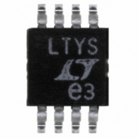
LT1801IMS8#TR Linear Technology, LT1801IMS8#TR Datasheet - Page 20

LT1801IMS8#TR
Manufacturer Part Number
LT1801IMS8#TR
Description
IC OPAMP R-R I/O DUAL LP 8MSOP
Manufacturer
Linear Technology
Datasheet
1.LT1801CS8PBF.pdf
(20 pages)
Specifications of LT1801IMS8#TR
Amplifier Type
General Purpose
Number Of Circuits
2
Output Type
Rail-to-Rail
Slew Rate
20 V/µs
Gain Bandwidth Product
70MHz
Current - Input Bias
400nA
Voltage - Input Offset
700µV
Current - Supply
1.8mA
Current - Output / Channel
50mA
Voltage - Supply, Single/dual (±)
2.3 V ~ 12.6 V, ±1.15 V ~ 6.3 V
Operating Temperature
-40°C ~ 85°C
Mounting Type
Surface Mount
Package / Case
8-MSOP, Micro8™, 8-uMAX, 8-uSOP,
Lead Free Status / RoHS Status
Contains lead / RoHS non-compliant
-3db Bandwidth
-
Available stocks
Company
Part Number
Manufacturer
Quantity
Price
LT1801/LT1802
TYPICAL APPLICATION
Low Power High Voltage Amplifi er
Certain materials used in optical applications have charac-
teristics that change due to the presence and strength of a
DC electric fi eld. The voltage applied across these materials
should be precisely controlled to maintain desired proper-
ties, sometimes as high as 100’s of volts. The materials
are not conductive and represent a capacitive load.
The circuit of Figure 6 shows the LT1801 used in an ampli-
fi er capable of a 250V output swing and providing precise
DC output voltage. When no signal is present, the op
RELATED PARTS
PART NUMBER DESCRIPTION
LT1399
LT1498/LT1499 Dual/Quad 10MHz, 6V/μs Rail-to-Rail Input and Output C-Load
LT1630/LT1631 Dual/Quad 30MHz, 10V/μs Rail-to-Rail Input and Output Op Amps
LT1800
LT1806/LT1807 Single/Dual 325MHz, 140V/μs Rail-to-Rail Input and Output Op Amps
LT1809/LT1810
C-Load is a trademark of Linear Technology Corporation
20
V
IN
150V
8pF
C2
0.1μF
R2
2k
R1
2k
Linear Technology Corporation
1630 McCarthy Blvd., Milpitas, CA 95035-7417
(408) 432-1900
R3
200k
+
–
1/2 LT1801
Triple 300MHz Current Feedback Amplifi er
80MHz, 25V/μs Low Power Rail-to-Rail Input/Output Precision Op Amp
Single/Dual 180MHz Rail-to-Rail Input/Output Op Amps
Figure 6. Low Power, High Voltage Amplifi er
39pF
5V
C1
●
FAX: (408) 434-0507
Q1
Q3
5V
10k
10k
R4
R5
2k
2k
Q5
Q7
Q4
Q2
4.99k
4.99k
–130V
130V
5V
R6
2k
R7
2k
●
Q6
Q8
18012 F06
1k
1k
www.linear.com
A
±130V SUPPLY I
OUTPUT SWING = ±128.8V
OUTPUT OFFSET ≅ 20mV
OUTPUT SHORT-CIRCUIT CURRENT ≅ 3mA
10% TO 90% RISE TIME ≅ 8μs, 200V OUTPUT STEP
SMALL-SIGNAL BANDWIDTH ≅ 150kHz
Q1, Q2, Q7, Q8: ON SEMI MPSA42
Q3, Q4, Q5, Q6: ON SEMI MPSA92
V
V
OUT
= V
MATERIAL UNDER
ELECTRIC FIELD
100pF
OUT
/V
IN
= –100
Q
= 130μA
amp output sits at about mid-supply. Transistors Q1 and
Q3 create bias voltages for Q2 and Q4, which are forced
into a low quiescent current by degeneration resistors
R4 and R5. When a transient signal arrives at V
amp output moves and causes the current in Q2 or Q4
to change depending on the signal polarity. The current,
limited by the clipping of the LT1801 output and the 3kΩ
of total emitter degeneration, is mirrored to the output
devices to drive the capacitive load. The LT1801 output
then returns to near mid-supply, providing the precise DC
output voltage to the load. The attention to limit the current
of the output devices minimizes power dissipation thus
allowing for dense layout, and inherits better reliability.
Figure 7 shows the time domain response of the amplifi er
providing a 200V output swing into a 100pF load.
™
Op Amps High DC Accuracy, 475μV V
COMMENTS
0.1dB Gain Flatness to 150MHz, Shutdown
High DC Accuracy, 525μV V
Current, Max Supply Current 4.4mA per Amplifi er
Single Version of LT1801/LT1802
High DC Accuracy, 550μV V
Low Distortion –80dB at 5MHz, Power-Down (LT1806)
350V/μs Slew Rate, Low Distortion –90dBc at 5MHz,
Power-Down (LT1809)
50V/DIV
2V/DIV
V
OUT
V
IN
Figure 7. Large-Signal Time Domain
Response of the Amplifi er
© LINEAR TECHNOLOGY CORPORATION 2002
OS(MAX)
OS(MAX)
OS(MAX)
10μs/DIV
LT 0309 REV C • PRINTED IN USA
, Low Noise 3.5nV/√Hz,
, 4μV/°C Max Drift
, 70mA Output
IN
, the op
18012 F07
18012fc


