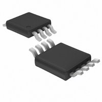
LT1801IMS8 Linear Technology, LT1801IMS8 Datasheet - Page 8

LT1801IMS8
Manufacturer Part Number
LT1801IMS8
Description
IC OPAMP R-R IN/OUT DUAL 8-MSOP
Manufacturer
Linear Technology
Datasheet
1.LT1801CS8PBF.pdf
(20 pages)
Specifications of LT1801IMS8
Amplifier Type
General Purpose
Number Of Circuits
2
Output Type
Rail-to-Rail
Slew Rate
20 V/µs
Gain Bandwidth Product
70MHz
Current - Input Bias
400nA
Voltage - Input Offset
700µV
Current - Supply
1.8mA
Current - Output / Channel
50mA
Voltage - Supply, Single/dual (±)
2.3 V ~ 12.6 V, ±1.15 V ~ 6.3 V
Operating Temperature
-40°C ~ 85°C
Mounting Type
Surface Mount
Package / Case
8-MSOP, Micro8™, 8-uMAX, 8-uSOP,
Lead Free Status / RoHS Status
Contains lead / RoHS non-compliant
-3db Bandwidth
-
Available stocks
Company
Part Number
Manufacturer
Quantity
Price
Company:
Part Number:
LT1801IMS8
Manufacturer:
LT
Quantity:
10 000
Part Number:
LT1801IMS8
Manufacturer:
LINEAR/凌特
Quantity:
20 000
Company:
Part Number:
LT1801IMS8#PBF
Manufacturer:
LT
Quantity:
1 036
Part Number:
LT1801IMS8#PBF
Manufacturer:
LINEAR/凌特
Quantity:
20 000
Company:
Part Number:
LT1801IMS8#TRPBF
Manufacturer:
VISHAY
Quantity:
6 217
Part Number:
LT1801IMS8#TRPBF
Manufacturer:
LINEAR/凌特
Quantity:
20 000
LT1801/LT1802
ELECTRICAL CHARACTERISTICS
of – 40°C < T
SYMBOL PARAMETER
V
I
I
A
CMRR
PSRR
V
V
I
I
GBW
SR
Note 1: Stresses beyond those listed under Absolute Maximum Ratings
may cause permanent damage to the device. Exposure to any Absolute
Maximum Rating condition for extended periods may affect device
reliability and lifetime.
Note 2: The inputs are protected by back-to-back diodes. If the differential
input voltage exceeds 1.4V, the input current should be limited to less than
10mA. It is not 100% tested.
Note 3: A heat sink may be required to keep the junction temperature
below the absolute maximum rating when the output is shorted
indefi nitely.
Note 4: The LT1801C/LT1801I and LT1802C/LT1802I are guaranteed
functional over the temperature range of – 40°C to 85°C.
Note 5: The LT1801C/LT1802C are guaranteed to meet specifi ed
performance from 0°C to 70°C. The LT1801C/LT1802C are designed,
characterized and expected to meet specifi ed performance from
–40°C to 85°C but are not tested or QA sampled at these temperatures.
The LT1801I/LT1802I are guaranteed to meet specifi ed performance from
–40°C to 85°C.
8
B
OS
SC
S
OS
VOL
OL
OH
TC
Input Offset Voltage Drift (Note 8)
Input Bias Current
Input Bias Current Match
(Channel-to-Channel) (Note 9)
Input Offset Current
Large-Signal Voltage Gain
Common Mode Rejection Ratio
CMRR Match (Channel-to-Channel) (Note 9) V
Input Common Mode Range
Power Supply Rejection Ratio
PSRR Match (Channel-to-Channel) (Note 9) V
Output Voltage Swing Low (Note 7)
Output Voltage Swing High (Note 7)
Short-Circuit Current
Supply Current per Amplifi er
Gain Bandwidth Product
Slew Rate
A
< 85°C. V
S
= ±5V, V
CM
= 0V, V
OUT
= 0V, unless otherwise noted. (Note 5)
CONDITIONS
V
V
V
V
V
V
V
V
V
V
No Load
I
I
No Load
I
I
Frequency = 2MHz
A
Measured at V
SINK
SINK
SOURCE
SOURCE
O
O
V
CM
CM
CM
CM
CM
CM
CM
CM
S
S
+
+
= – 1, R
= –4V to 4V, R
= –1V to 1V, R
= 2.5V to 10V, V
= 2.5V to 10V, V
= V
= V
= V
= V
= V
= V
= V
= V
= 5mA
= 10mA
S
S
S
S
S
S
S
S
= 5mA
= 10mA
–
+
–
+
–
+
–
–
The
L
+ 1V
– 0.2V
+ 1V
– 0.2V
+ 1V
– 0.2V
to 3.5V
to 3.5V
= 1k, V
O
l
= ±2V
L
denotes the specifi cations which apply over the temperature range
L
O
= 100Ω
= 1k
S
S
= ±4V,
–
–
Note 6: Minimum supply voltage is guaranteed by power supply rejection
ratio test.
Note 7: Output voltage swings are measured between the output and
power supply rails.
Note 8: This parameter is not 100% tested.
Note 9: Matching parameters are the difference between amplifi ers A
and D and between B and C on the LT1802; between the two amplifi ers
on the LT1801.
Note 10: Thermal resistance (θ
metal connected to the package. The specifi ed values are for short
traces connected to the leads. If desired, the thermal resistance can be
substantially reduced by connecting Pin 4 of the SO-8 and MS8, Pin 11 of
the SO-14 or the underside metal of the DD package to a larger metal area
(V
= 0V
= 0V
S
–
trace).
l
l
l
l
l
l
l
l
l
l
l
l
l
l
l
l
l
l
l
l
l
l
l
l
JA
) varies with the amount of PC board
MIN
12.5
12.5
V
81
75
73
67
2
S
–
TYP
450
300
104
104
110
180
150
2.6
1.5
50
25
25
25
25
55
90
90
20
30
30
65
15
5
2250
MAX
400
450
700
350
350
100
275
400
350
700
V
110
4.5
5
S
+
UNITS
18012fc
μV/°C
V/mV
V/mV
MHz
V/μs
mA
mA
mV
mV
mV
mV
mV
mV
nA
nA
nA
nA
nA
nA
dB
dB
dB
dB
V


