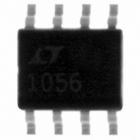
LT1056S8 Linear Technology, LT1056S8 Datasheet - Page 10

LT1056S8
Manufacturer Part Number
LT1056S8
Description
IC PREC OP-AMP JFET HI-SPD 8SOIC
Manufacturer
Linear Technology
Datasheet
1.LT1055CN8PBF.pdf
(16 pages)
Specifications of LT1056S8
Amplifier Type
J-FET
Number Of Circuits
1
Slew Rate
14 V/µs
Gain Bandwidth Product
5.5MHz
Current - Input Bias
30pA
Voltage - Input Offset
500µV
Current - Supply
5mA
Voltage - Supply, Single/dual (±)
±5 V ~ 18 V
Operating Temperature
0°C ~ 70°C
Mounting Type
Surface Mount
Package / Case
8-SOIC (3.9mm Width)
Lead Free Status / RoHS Status
Contains lead / RoHS non-compliant
Output Type
-
Current - Output / Channel
-
-3db Bandwidth
-
Available stocks
Company
Part Number
Manufacturer
Quantity
Price
Company:
Part Number:
LT1056S8
Manufacturer:
LINEAR
Quantity:
3
Part Number:
LT1056S8
Manufacturer:
LINEAR/凌特
Quantity:
20 000
Company:
Part Number:
LT1056S8#PBF
Manufacturer:
LT
Quantity:
759
APPLICATIONS
LT1055/LT1056
The voltage noise spectrum is characterized by a low 1/f
corner in the 20Hz to 30Hz range, significantly lower than
on other competitive JFET input op amps. Of particular
interest is the fact that with any JFET IC amplifier, the
frequency location of the 1/f corner is proportional to the
square root of the internal gate leakage currents and,
therefore, noise doubles every 20°C. Furthermore, as
illustrated in the noise versus chip temperature curves,
the 0.1Hz to 10Hz peak-to-peak noise is a strong function
of temperature, while wideband noise (f
practically unaffected by temperature.
Consequently, for optimum low frequency noise, chip
temperature should be minimized. For example, operating
an LT1056 at ±5V supplies or with a 20°C/W case-to-
ambient heat sink reduces 0.1Hz to 10Hz noise from
typically 2.5µV
the noise of an LT1055 will be 1.8µV
of its lower power dissipation and chip temperature.
High Speed Operation
Settling time is measured in the test circuit shown. This
test configuration has two features which eliminate prob-
lems common to settling time measurments: (1) probe
(5V MIN STEP)
10
PULSE GEN
INPUT
2k
2k
50Ω
2W
P-P
(±15V, free-air) to 1.5µV
U
–15V
–15V
+
INFORMATION
0.01 DISC
0.01 DISC
0.01 DISC
10µF
SOLID
TANTALUM
U
15V
15V
W
+
+
+
+
P-P
10µF
SOLID
TANTALUM
0.01 DISC
10µF
SOLID
TANTALUM
10µF
SOLID TANTALUM
typically because
15k
15k
15k
15k
P-P
0
= 1kHz) is
. Similiarly,
U
Settling Time Test Circuit
10pF (TYPICAL)
–
+
LT1055
LT1056
AMPLIFIER
10k
UNDER
TEST
capacitance is isolated from the “false summing” node,
and (2) it does not require a “flat top” input pulse since the
input pulse is merely used to steer current through the
diode bridges. For more details, please see Application
Note 10.
As with most high speed amplifiers, care should be
taken with supply decoupling, lead dress and component
placement.
When the feedback around the op amp is resistive (R
pole will be created with R
capacitance (R
(C
with R
excess phase shift and even oscillation. A small capacitor
(C
(C
completely removed.
IN
F
S
) in parallel with R
+ C
≈ 4pF). In low closed-loop gain configurations and
S
= 1N4148
10k
and R
IN
AUT OUTPUT
) = R
HP5082-8210
HEWLETT
PACKARD
R
F
S
S
, C
in the kilohm range, this pole can create
F
C
S
F
, the effect of the feedback pole is
), and the amplifier input capacitance
C
F
S
eliminates this problem. With R
–
+
F
–15V
, the source resistance and
15V
1/2
U440
1/2
U440
50Ω
C
R
100Ω
DC ZERO
C
F
F
IN
LT1055/56 AI03
–15V
15V
2N160
2N3866
OUTPUT
4.7k
4.7k
–15V
15V
2N3866
2N5160
3Ω
3Ω
OUTPUT
TO SCOPE
LT1055/56 AI04
10556fc
F
), a
S


