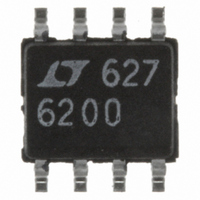
LT6200CS8 Linear Technology, LT6200CS8 Datasheet - Page 7

LT6200CS8
Manufacturer Part Number
LT6200CS8
Description
IC OPAMP R-R I/O 165MHZ 8-SOIC
Manufacturer
Linear Technology
Datasheet
1.LT6200CS6TRMPBF.pdf
(26 pages)
Specifications of LT6200CS8
Amplifier Type
Buffer
Number Of Circuits
1
Output Type
Rail-to-Rail
Slew Rate
50 V/µs
Gain Bandwidth Product
165MHz
Current - Input Bias
23µA
Voltage - Input Offset
2500µV
Current - Supply
20mA
Current - Output / Channel
90mA
Voltage - Supply, Single/dual (±)
2.5 V ~ 12.6 V, ±1.25 V ~ 6.3 V
Operating Temperature
0°C ~ 70°C
Mounting Type
Surface Mount
Package / Case
8-SOIC (3.9mm Width)
Lead Free Status / RoHS Status
Contains lead / RoHS non-compliant
-3db Bandwidth
-
Available stocks
Company
Part Number
Manufacturer
Quantity
Price
Company:
Part Number:
LT6200CS8
Manufacturer:
LT
Quantity:
10 000
Part Number:
LT6200CS8
Manufacturer:
LTNEAR
Quantity:
20 000
Company:
Part Number:
LT6200CS8#PBF
Manufacturer:
LT
Quantity:
2 010
Part Number:
LT6200CS8#PBF
Manufacturer:
LINEAR/凌特
Quantity:
20 000
Company:
Part Number:
LT6200CS8-10
Manufacturer:
LT
Quantity:
10 000
Company:
Part Number:
LT6200CS8-10#PBF
Manufacturer:
LT
Quantity:
2 780
Part Number:
LT6200CS8-10#PBF
Manufacturer:
LINEAR/凌特
Quantity:
20 000
Company:
Part Number:
LT6200CS8-5
Manufacturer:
LT
Quantity:
10 000
Part Number:
LT6200CS8-5
Manufacturer:
LINEAR/凌特
Quantity:
20 000
Part Number:
LT6200CS8-5#TRPBF
Manufacturer:
LINEAR/凌特
Quantity:
20 000
ELECTRICAL CHARACTERISTICS
Excludes the LT6201 in the DD package (Note 3).
SYMBOL
I
ΔI
I
e
i
C
A
CMRR
PSRR
V
V
I
I
I
V
V
t
t
GBW
SR
FPBW
t
n
B
OS
SC
S
SHDN
ON
OFF
S
n
VOL
IN
OL
OH
L
H
B
PARAMETER
Input Bias Current
I
I
Input Offset Current
Input Noise Voltage
Input Noise Voltage Density
Input Noise Current Density, Balanced Source
Input Resistance
Input Capacitance
Large-Signal Gain
Common Mode Rejection Ratio
CMRR Match (Channel-to-Channel) (Note 11)
Power Supply Rejection Ratio
PSRR Match (Channel-to-Channel) (Note 6)
Output Voltage Swing LOW (Note 7)
Output Voltage Swing HIGH (Note 7)
Short-Circuit Current
Supply Current per Amplifi er
Disabled Supply Current per Amplifi er
SHDN Pin Current
V
V
Shutdown Output Leakage Current
Turn-On Time
Turn-Off Time
Gain Bandwidth Product
Slew Rate
Full Power Bandwidth (Note 9)
Setting Time (LT6200, LT6201)
B
B
SHDN
SHDN
Shift
Match (Channel-to-Channel) (Note 11)
Pin Input Voltage LOW
Pin Input Voltage HIGH
Unbalanced Source
CONDITIONS
V
V
V
V
V
V
V
V
0.1Hz to 10Hz
f = 100kHz
f = 10kHz
f = 10kHz
f = 10kHz
Common Mode
Differential Mode
Common Mode
Differential Mode
V
V
V
V
V
V
V
No Load
I
I
No Load
I
I
V
V
V
V
V
Frequency = 1MHz
LT6200-5
LT6200-10
A
A
LT6200-5
LT6200-10
V
0.1%, V
SINK
SINK
SOURCE
SOURCE
CM
CM
CM
CM
CM
CM
CM
CM
O
O
CM
CM
CM
S
S
SHDN
SHDN
SHDN
SHDN
SHDN
OUT
V
V
T
= ±1.25V to ±5V
= ±1.25V to ±5V
= ±4.5V, R
= ±2V, R
= –1, R
= –10, R
A
= Half Supply
= V
= V
= V
= V
= Half Supply
= V
= V
= V
= –2V to 2V
= –2V to 2V
= 5mA
= 20mA
= 3V
= 25°C, V
= 0.3V
= 0.3V
= 0.3V
= 0.3V to 4.5V, R
= 4.5V to 0.3V, R
+
+
STEP
–
–
–
–
–
= 5mA
= 20mA
to V
to V
to V
P-P
L
L
L
= 1k, V
= 1, R
= 100
= 1k, V
(LT6200-10)
+
+
+
L
= 1k
S
= ±5V, V
L
O
O
= 1k
= 4V
= 4V
L
L
= 100Ω, V
= 100Ω, V
CM
= V
OUT
S
S
= 5V
= 5V
= 0V, V
LT6200-10/LT6201
LT6200/LT6200-5
SHDN
V
1060
MIN
– 40
+
–50
115
±60
110
530
175
315
15
68
75
80
60
65
35
33
= OPEN, unless otherwise noted.
–0.5
1600
0.95
0.57
TYP
–10
–23
600
200
100
105
100
150
110
225
±90
200
130
180
165
800
250
450
140
0.2
1.3
1.4
2.2
3.5
2.1
3.1
4.2
1.6
0.1
31
26
96
68
12
55
70
20
50
47
8
1
3
MAX
110
290
130
210
420
280
2.3
2.1
0.3
18
68
12
50
23
75
6
7
7
nV/√Hz
nV/√Hz
pA/√Hz
pA/√Hz
UNITS
62001fd
nV
V/mV
V/mV
7
MHz
MHz
MHz
V/μs
V/μs
V/μs
MHz
MΩ
mV
mV
mV
mV
mV
mV
mA
mA
mA
kΩ
P-P
μA
μA
μA
μA
μA
μA
μA
μA
dB
dB
dB
dB
dB
μA
μA
pF
pF
ns
ns
ns
V
V


