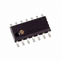
MCP6064-E/SL Microchip Technology, MCP6064-E/SL Datasheet - Page 3

MCP6064-E/SL
Manufacturer Part Number
MCP6064-E/SL
Description
IC OPAMP PREC 6.0V 60UA 14-SOIC
Manufacturer
Microchip Technology
Specifications of MCP6064-E/SL
Slew Rate
0.25 V/µs
Amplifier Type
General Purpose
Number Of Circuits
4
Output Type
Rail-to-Rail
Gain Bandwidth Product
730kHz
Current - Input Bias
1pA
Voltage - Input Offset
150µV
Current - Supply
60µA
Current - Output / Channel
27mA
Voltage - Supply, Single/dual (±)
1.8 V ~ 6 V
Operating Temperature
-40°C ~ 125°C
Mounting Type
Surface Mount
Package / Case
14-SOIC (3.9mm Width), 14-SOL
Op Amp Type
Precision
No. Of Amplifiers
4
Bandwidth
730kHz
Supply Voltage Range
1.8V To 6V
Amplifier Case Style
SOIC
No. Of Pins
14
Number Of Channels
4
Voltage Gain Db
115 dB
Common Mode Rejection Ratio (min)
72 dB
Input Offset Voltage
0.15 mV
Operating Supply Voltage
3 V, 5 V
Maximum Operating Temperature
+ 125 C
Mounting Style
SMD/SMT
Minimum Operating Temperature
- 40 C
Lead Free Status / RoHS Status
Lead free / RoHS Compliant
-3db Bandwidth
-
Lead Free Status / Rohs Status
Details
Available stocks
Company
Part Number
Manufacturer
Quantity
Price
Company:
Part Number:
MCP6064-E/SL
Manufacturer:
MICROCHIP
Quantity:
12 000
Part Number:
MCP6064-E/SL
Manufacturer:
MICROCHIP/微芯
Quantity:
20 000
1.0
1.1
V
Current at Input Pins .....................................................±2 mA
Analog Inputs (V
All Other Inputs and Outputs ......... V
Difference Input Voltage ...................................... |V
Output Short-Circuit Current .................................continuous
Current at Output and Supply Pins ............................±30 mA
Storage Temperature ....................................-65°C to +150°C
Maximum Junction Temperature (T
ESD protection on all pins (HBM; MM) ................ ≥ 4 kV; 400V
1.2
DC ELECTRICAL SPECIFICATIONS
© 2010 Microchip Technology Inc.
Electrical Characteristics: Unless otherwise indicated, V
V
Input Offset
Input Offset Voltage
Input Offset Drift with Temperature
Power Supply Rejection Ratio
Input Bias Current and Impedance
Input Bias Current
Input Offset Current
Common Mode Input Impedance
Differential Input Impedance
Common Mode
Common Mode Input Voltage Range
Common Mode Rejection Ratio
Note 1:
DD
OUT
– V
≈ V
SS
ELECTRICAL
CHARACTERISTICS
Absolute Maximum Ratings †
Specifications
........................................................................7.0V
DD
Figure 2-13
/2, V
Parameters
IN
+
L
, V
= V
IN
-
)†† .......... V
DD
shows how V
/2 and R
J
) .......................... +150°C
SS
SS
L
= 10 kΩ to V
– 1.0V to V
– 0.3V to V
CMR
ΔV
ΔV
CMRR
PSRR
V
V
changed across temperature.
Z
Sym
V
OS
OS
Z
I
DIFF
CMR
CMR
OS
I
I
I
CM
OS
B
B
B
/ΔT
/ΔT
DD
DD
DD
L
+ 1.0V
+ 0.3V
A
A
– V
. (Refer to
SS
V
V
SS
|
SS
-150
Min
70
72
74
72
74
—
—
—
—
—
—
—
—
−0.15
−0.3
DD
Figure
= +1.8V to +6.0V, V
† Notice: Stresses above those listed under “Absolute
Maximum Ratings” may cause permanent damage to
the device. This is a stress rating only and functional
operation of the device at those or any other conditions
above those indicated in the operational listings of this
specification is not implied. Exposure to maximum
rating conditions for extended periods may affect
device reliability.
†† See
10
10
1100
±1.5
±4.0
±1.0
±1.0
Typ
87
60
89
91
87
89
—
—
—
13
13
1-1).
||6
||6
4.1.2 “Input Voltage Limits”
V
V
DD
DD
+150
5000
Max
100
—
—
—
—
—
—
—
—
—
—
—
+0.15
+0.3
SS
= GND, T
µV/°C T
µV/°C T
MCP6061/2/4
Units
Ω||pF
Ω||pF
µV
dB
pA
pA
pA
pA
dB
dB
dB
dB
V
V
V
V
V
V
V
T
T
V
V
V
V
V
V
V
V
V
V
A
A
A
A
A
DD
CM
DD
DD
CM
DD
DD
CM
DD
CM
DD
CM
DD
CM
DD
= -40°C to +85°C,
= +85°C to +125°C,
= +25°C, V
= +85°C
= +125°C
= 1.8V
= 6.0V
= 1.8V
= 6.0V
= 6.0V
= 6.0V
= 3.0V,
= 3.0V, V
= 3.0V, V
= -0.15V to 1.95V,
= -0.3V to 6.3V,
= 3.0V to 6.3V,
= -0.3V to 3.0V,
= V
= V
Conditions
DD
SS
DS22189B-page 3
/3
(Note
(Note
CM
CM
CM
= V
= V
= V
1)
1)
DD
DD
DD
/2,
/3
/3


