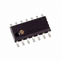
MCP6144-I/SL Microchip Technology, MCP6144-I/SL Datasheet - Page 13

MCP6144-I/SL
Manufacturer Part Number
MCP6144-I/SL
Description
IC OPAMP 1.4V QUAD R-R 14-SOIC
Manufacturer
Microchip Technology
Specifications of MCP6144-I/SL
Slew Rate
0.003 V/µs
Operating Temperature
-40°C ~ 85°C
Amplifier Type
General Purpose
Number Of Circuits
4
Output Type
Rail-to-Rail
Gain Bandwidth Product
100kHz
Current - Input Bias
1pA
Voltage - Input Offset
3000µV
Current - Supply
0.6µA
Current - Output / Channel
20mA
Voltage - Supply, Single/dual (±)
1.4 V ~ 6 V
Mounting Type
Surface Mount
Package / Case
14-SOIC (3.9mm Width), 14-SOL
Op Amp Type
General Purpose
No. Of Amplifiers
4
Bandwidth
100kHz
Supply Voltage Range
1.4V To 5.5V
Amplifier Case Style
SOIC
No. Of Pins
14
Number Of Channels
4
Voltage Gain Db
115 dB
Common Mode Rejection Ratio (min)
60 dB
Input Offset Voltage
3 mV
Operating Supply Voltage
3 V, 5 V
Supply Current
0.004 mA
Maximum Operating Temperature
+ 85 C
Mounting Style
SMD/SMT
Minimum Operating Temperature
- 40 C
Lead Free Status / RoHS Status
Lead free / RoHS Compliant
-3db Bandwidth
-
Lead Free Status / Rohs Status
Details
Available stocks
Company
Part Number
Manufacturer
Quantity
Price
Company:
Part Number:
MCP6144-I/SL
Manufacturer:
MICROCHIP
Quantity:
12 000
EQUATION 4-2:
In order for the amplifiers to be stable, the noise gain
should meet the specified minimum noise gain. Note
that a noise gain of G
non-inverting signal gain of G = +10 V/V, or to an
inverting signal gain of G = -9 V/V.
FIGURE 4-2:
Gain Configuration.
FIGURE 4-3:
Gain Configuration.
Figure 4-4 shows a unity gain buffer and Miller integra-
tor
MCP6141/2/3/4 family. Note that the capacitor makes
the integrator circuit reach unity gain at high
frequencies, which makes these op amps unstable.
FIGURE 4-4:
the MCP6141/2/3/4 Family.
© 2005 Microchip Technology Inc.
Unity Gain Buffer
Miller Integrator
that
V
V
IN
IN
V
V
IN
IN
are
R
R
R
R
G
IN
IN
G
G
N
unstable
R
MCP614X
=
Noise Gain for Non-inverting
Noise Gain for Inverting
Typical Unstable Circuits for
1
MCP614X
MCP614X
N
+
= +10 V/V corresponds to a
MCP614X
------ -
R
R
F
G
R
R
when
F
F
C
10 V/V
used
V
OUT
V
V
with
OUT
OUT
V
OUT
the
4.4.2
Driving large capacitive loads can cause stability
problems for voltage feedback op amps. As the load
capacitance increases, the feedback loop’s phase
margin decreases and the closed-loop bandwidth is
reduced. This produces gain peaking in the frequency
response, with overshoot and ringing in the step
response. A unity gain buffer (G = +1) is the most
sensitive to capacitive loads, though all gains show the
same general behavior.
When driving large capacitive loads with these op
amps (e.g., > 60 pF when G = +10), a small series
resistor at the output (R
feedback loop’s phase margin (stability) by making the
output load resistive at higher frequencies. The band-
width will be generally lower than the bandwidth with no
capacitive load.
FIGURE 4-5:
stabilizes large capacitive loads.
Figure 4-6 gives recommended R
ent capacitive loads and gains. The x-axis is the nor-
malized load capacitance (C
circuit’s noise gain. For non-inverting gains, G
Signal Gain are equal. For inverting gains, G
1+|Signal Gain| (e.g., -9 V/V gives G
FIGURE 4-6:
for Capacitive Loads.
After selecting R
resulting frequency response peaking and step
response overshoot. Modify R
response is reasonable. Bench evaluation and simula-
tions with the MCP6141/2/3/4 SPICE macro model are
helpful.
V
A
100,000
10,000
1,000
100k
10k
1k
1.E+00
R
V
1p
G
CAPACITIVE LOADS
B
Normalized Load Capacitance; C
MCP6141/2/3/4
ISO
MCP614X
for your circuit, double check the
1.E+01
Output Resistor, R
10p
Recommended R
R
ISO
F
in Figure 4-5) improves the
L
/G
ISO
N
G
G
G
1.E+02
ISO
100p
), where G
N
N
N
R
’s value until the
C
= +10
= +20
N
DS21668B-page 13
ISO
t t +50
values for differ-
L
= +10 V/V).
L
/G
ISO
ISO
N
(F)
N
1.E+03
N
Values
and the
V
1n
is the
OUT
N
is


