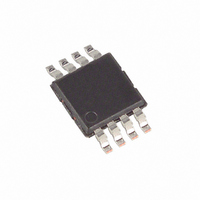
MAX4215EUA+ Maxim Integrated Products, MAX4215EUA+ Datasheet - Page 9

MAX4215EUA+
Manufacturer Part Number
MAX4215EUA+
Description
IC BUFFER R-R W/ENABLE 8-UMAX
Manufacturer
Maxim Integrated Products
Datasheet
1.MAX4222ESD.pdf
(16 pages)
Specifications of MAX4215EUA+
Amplifier Type
Buffer
Number Of Circuits
1
Output Type
Rail-to-Rail
Slew Rate
600 V/µs
-3db Bandwidth
230MHz
Current - Input Bias
5.4µA
Voltage - Input Offset
4000µV
Current - Supply
5.5mA
Current - Output / Channel
120mA
Voltage - Supply, Single/dual (±)
3.15 V ~ 11 V, ±1.575 V ~ 5.5 V
Operating Temperature
-40°C ~ 85°C
Mounting Type
Surface Mount
Package / Case
8-MSOP, Micro8™, 8-uMAX, 8-uSOP,
Lead Free Status / RoHS Status
Lead free / RoHS Compliant
Gain Bandwidth Product
-
The MAX4214/MAX4215/MAX4217/MAX4219/MAX4222
are single-supply, rail-to-rail output, voltage-feedback,
closed-loop buffers that employ current-feedback tech-
niques to achieve 600V/µs slew rates and 230MHz
bandwidths. These buffers use internal 500
to provide a preset closed-loop gain of 2V/V in the non-
inverting configuration or -1V/V in the inverting configu-
ration. Excellent harmonic distortion and differential
gain/phase performance make them an ideal choice for
a wide variety of video and RF signal-processing appli-
cations.
Local feedback around the buffer’s output stage
ensures low output impedance, which reduces gain
sensitivity to load variations. This feedback also pro-
duces demand-driven current bias to the output tran-
sistors for ±120mA drive capability, while constraining
total supply current to less than 7mA.
These devices operate from a single 3.15V to 11V
power supply or from dual supplies of ±1.575V to
±5.5V. For single-supply operation, bypass the V
to ground with a 0.1µF capacitor as close to the pin as
possible. If operating with dual supplies, bypass each
supply with a 0.1µF capacitor.
Each buffer in the MAX4214 family can be configured
for a voltage gain of 2V/V or -1V/V. For a gain of 2V/V,
ground the inverting terminal. Use the noninverting ter-
minal as the signal input of the buffer (Figure 1a).
Grounding the noninverting terminal and using the
inverting terminal as the signal input configures the
buffer for a gain of -1V/V (Figure 1b).
Figure 1a. Noninverting Gain Configuration (A
________________Detailed Description
___________Applications Information
IN
R
TIN
Closed-Loop, Rail-to-Rail Buffers with Enable
IN+
IN-
500
500
_______________________________________________________________________________________
Selecting Gain Configuration
MAX42_ _
OUT
High-Speed, Single-Supply, Gain of 2,
R
TO
Power Supplies
V
= +2V/V)
resistors
CC
R
O
OUT
pin
Since the inverting input exhibits a 500
ance, terminate the input with a 56
figured for an inverting gain in 50
(terminate with 88
input with a 49.9
Output terminating resistors should directly match
cable impedances in either configuration.
Maxim recommends using microstrip and stripline tech-
niques to obtain full bandwidth. To ensure the PC
board does not degrade the buffer’s performance,
design it for a frequency greater than 1GHz. Pay care-
ful attention to inputs and outputs to avoid large para-
sitic capacitance. Whether or not you use a constant-
impedance board, observe the following guidelines
when designing the board:
The MAX4214 family’s input range extends from
(V
increases the dynamic range for single-supply applica-
tions. The outputs drive a 2k
the power-supply rails. With smaller resistive loads, the
output swing is reduced as shown in the Electrical
Characteristics and Typical Operating Characteristics.
Figure 1b. Inverting Gain Configuration (A
IN
R
R
EE
TIN
Don’t use wire-wrapped boards. They are too induc-
tive.
Don’t use IC sockets. They increase parasitic capac-
itance and inductance.
Use surface-mount instead of through-hole compo-
nents for better high-frequency performance.
Use a PC board with at least two layers; it should be
as free from voids as possible.
Keep signal lines as short and as straight as possi-
ble. Do not make 90° turns; round all corners.
S
Input Voltage Range and Output Swing
- 100mV) to (V
IN+
IN-
500
500
in 75
CC
resistor in the noninverting case.
MAX42_ _
- 2.25V). Input ground sensing
applications). Terminate the
OUT
Layout Techniques
load to within 60mV of
R
TO
V
resistor when con-
= -1V/V)
applications
input imped-
R
O
OUT
9


