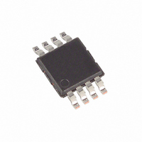
MAX4203EUA+ Maxim Integrated Products, MAX4203EUA+ Datasheet - Page 8

MAX4203EUA+
Manufacturer Part Number
MAX4203EUA+
Description
IC BUFFER OPEN LOOP 8-UMAX
Manufacturer
Maxim Integrated Products
Datasheet
1.MAX4200ESA.pdf
(14 pages)
Specifications of MAX4203EUA+
Amplifier Type
Buffer
Number Of Circuits
2
Slew Rate
4200 V/µs
-3db Bandwidth
530MHz
Current - Input Bias
800nA
Voltage - Input Offset
1000µV
Current - Supply
2.2mA
Current - Output / Channel
90mA
Voltage - Supply, Single/dual (±)
±4 V ~ 5.5 V
Operating Temperature
-40°C ~ 85°C
Mounting Type
Surface Mount
Package / Case
8-MSOP, Micro8™, 8-uMAX, 8-uSOP,
Number Of Channels
2
Voltage Gain Db
0.35 dB
Input Offset Voltage
1 mV
Maximum Power Dissipation
330 mW
Maximum Operating Temperature
+ 85 C
Mounting Style
SMD/SMT
Maximum Dual Supply Voltage
+/- 5.5 V
Minimum Operating Temperature
- 40 C
Lead Free Status / RoHS Status
Lead free / RoHS Compliant
Output Type
-
Gain Bandwidth Product
-
Lead Free Status / Rohs Status
Details
Ultra-High-Speed, Low-Noise, Low-Power,
SOT23 Open-Loop Buffers
The MAX4200–MAX4205 wide-band, open-loop buffers
feature high slew rates, high output current, low
2.1nV√Hz voltage-noise density, and excellent capaci-
tive-load-driving capability. The MAX4200/MAX4203
are single/dual buffers with up to 660MHz bandwidth,
230MHz 0.1dB gain flatness, and a 4200V/µs slew rate.
The MAX4201/MAX4204 single/dual buffers with inte-
grated 50Ω output termination resistors, up to 780MHz
bandwidth, 280MHz gain flatness, and a 4200V/µs slew
rate, are ideally suited for driving high-speed signals
over 50Ω cables. The MAX4202/MAX4205 provide
bandwidths up to 720MHz, 230MHz gain flatness,
4200V/µs slew rate, and integrated 75Ω output termina-
tion resistors for driving 75Ω cables.
With an open-loop gain that is slightly less than +1V/V,
these devices do not have to be compensated with the
internal dominant pole (and its associated phase shift)
that is present in voltage-feedback devices. This fea-
ture allows the MAX4200–MAX4205 to achieve a nearly
constant group delay time of 405ps over their full fre-
quency range, making them well suited for a variety of
RF and IF signal-processing applications.
8
______________________________________________________________Pin Description
_______________Detailed Description
_______________________________________________________________________________________
MAX4200/MAX4201/MAX4202
SOT23-5
—
—
—
—
—
—
—
—
1
3
2
5
4
1, 2, 5, 8
PIN
SO
—
—
—
—
—
—
—
—
3
4
6
7
MAX4203
MAX4204
MAX4205
SO/µMAX
—
—
—
—
—
1
2
3
4
5
6
7
8
NAME
OUT1
OUT2
V
V
V
V
OUT
N.C.
V
V
IN1
IN2
These buffers operate with ±5V supplies and consume
only 2.2mA of quiescent supply current per buffer while
providing up to ±90mA of output current drive capability.
The MAX4200–MAX4205 operate with dual supplies
from ±4V to ±5.5V. Both V
bypassed to the ground plane with a 0.1µF capacitor
located as close to the device pin as possible.
Maxim recommends using microstrip and stripline tech-
niques to obtain full bandwidth. To ensure that the PC
board does not degrade the amplifier’s performance,
design it for a frequency greater than 6GHz. Pay care-
ful attention to inputs and outputs to avoid large para-
sitic capacitance. Whether or not you use a
constant-impedance board, observe the following
guidelines when designing the board:
• Do not use wire-wrap boards, because they are too
• Do not use IC sockets, because they increase para-
IN
CC2
CC1
EE1
EE2
CC
EE
__________Applications Information
inductive.
sitic capacitance and inductance.
No Connection. Not Internally Connected
Buffer Input
Buffer 1 Input
Buffer 1 Output
Negative Power Supply
Negative Power Supply for Buffer 1
Negative Power Supply for Buffer 2
Buffer 2 Input
Buffer 2 Output
Buffer Output
Positive Power Supply
Positive Power Supply for Buffer 2
Positive Power Supply for Buffer 1
FUNCTION
CC
Layout Techniques
and V
Power Supplies
EE
should be


