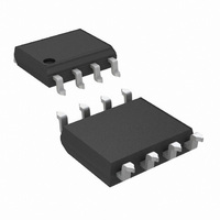
LMH6552MA/NOPB National Semiconductor, LMH6552MA/NOPB Datasheet - Page 15

LMH6552MA/NOPB
Manufacturer Part Number
LMH6552MA/NOPB
Description
IC AMP FULLY DIFF 1GHZ 8-SOIC
Manufacturer
National Semiconductor
Series
LMH®, PowerWise®r
Datasheet
1.LMH6552SDEVAL.pdf
(22 pages)
Specifications of LMH6552MA/NOPB
Amplifier Type
Differential
Number Of Circuits
1
Output Type
Differential
Slew Rate
3800 V/µs
-3db Bandwidth
1.5GHz
Current - Input Bias
60µA
Voltage - Input Offset
1500µV
Current - Supply
22.5mA
Current - Output / Channel
80mA
Voltage - Supply, Single/dual (±)
4.5 V ~ 12 V, ±2.25 V ~ 6 V
Operating Temperature
-40°C ~ 85°C
Mounting Type
Surface Mount
Package / Case
8-SOIC (3.9mm Width)
No. Of Amplifiers
1
Input Offset Voltage
16.5mV
Bandwidth
1.5GHz
Supply Voltage Range
4.5V To 12V
Supply Current
22.5mA
Amplifier Case Style
SOIC
No. Of Pins
8
Rohs Compliant
Yes
For Use With
LMH6552SDEVAL - BOARD EVALUATION FOR LMH6552
Lead Free Status / RoHS Status
Lead free / RoHS Compliant
Gain Bandwidth Product
-
Other names
*LMH6552MA
*LMH6552MA/NOPB
LMH6552MA
*LMH6552MA/NOPB
LMH6552MA
When using the LMH6552 in single-to-differential mode, the
complimentary output is forced to a phase inverted replica of
the driven output by the common mode feedback circuit as
opposed to being driven by its own complimentary input. Con-
sequently, as the driven input changes, the common mode
feedback action results in a varying common mode voltage at
the amplifier's inputs, proportional to the driving signal. Due
to the non-ideal common mode rejection of the amplifier's in-
put stage, a small common mode signal appears at the out-
puts which is superimposed on the differential output signal.
The ratio of the change in output common mode voltage to
output differential voltage is commonly referred to as output
balance error. The output balance error response of the
LMH6552 over frequency is shown in the Typical Perfor-
mance Characteristics section.
To match the input impedance of the circuit in
specified source resistance, R
The equations governing R
operation are also provided in
along with the source matching condition, must be solved it-
eratively to achieve the desired gain with the proper input
termination. Component values for several common gain con-
figurations in a 50Ω environment are given in Table 1. Typi-
cally R
Table 1. Gain Component Values for 50Ω System SOIC
Package
Table 2. Gain Component Values for 50Ω System LLP
Package
FIGURE 3. Single Ended Input with Differential Output
12 dB
12 dB
Gain
Gain
0 dB
6 dB
0 dB
6 dB
S
=50Ω while R
357Ω
357Ω
357Ω
275Ω
275Ω
275Ω
R
R
F
F
M
=R
S
76.8Ω
348Ω
169Ω
||R
54.9Ω
IN
255Ω
127Ω
R
R
and A
G
T.
S
G
, requires that R
Figure
V
for single-to-differential
56.2Ω
61.8Ω
76.8Ω
68.1Ω
107Ω
3. These equations,
59Ω
R
R
T
T
Figure 3
T
|| R
26.4Ω
27.6Ω
30.9Ω
26.7Ω
28.7Ω
34Ω
IN
R
R
30003510
M
M
= R
to a
S
.
15
The circuit shown in
eters for a single-to-differential configuration. The S-parame-
ter plots in the Typical Performance Curves are taken using
the recommended component values for 0 dB gain.
SINGLE SUPPLY OPERATION
Single supply operation is possible on supplies from 5V to
10V; however, as discussed earlier, AC input coupling is rec-
ommended for low supplies such as 5V due to input common
mode limitations. An example of an AC coupled, single sup-
ply, single-to-differential circuit is shown in
when AC coupling, both inputs need to be AC coupled irre-
spective of single-to-differential or differential-to-differential
configuration. For higher supply voltages DC coupling of the
inputs may be possible provided that the output common
mode DC level is set high enough so that the amplifier's inputs
and outputs are within their specified operating ranges.
FIGURE 4. Single Ended Input S-Parameter Test Circuit
FIGURE 5. AC Coupled for Single Supply Operation
Figure 4
(50Ω System)
was used to measure S-param-
Figure
www.national.com
5. Note that
30003509
30003554


