PA05 Cirrus Logic Inc, PA05 Datasheet - Page 4
PA05
Manufacturer Part Number
PA05
Description
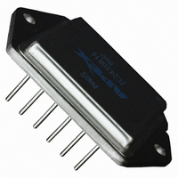
IC PWR AMP 100V 30A 12DIP
Manufacturer
Cirrus Logic Inc
Series
Apex Precision Power™r
Specifications of PA05
Amplifier Type
Power
Number Of Circuits
1
Slew Rate
100 V/µs
Gain Bandwidth Product
3MHz
Current - Input Bias
10pA
Voltage - Input Offset
5000µV
Current - Supply
90mA
Current - Output / Channel
30A
Voltage - Supply, Single/dual (±)
30 V ~ 100 V, ±15 V ~ 50 V
Operating Temperature
-25°C ~ 85°C
Mounting Type
Through Hole
Package / Case
12-DIP Module
Number Of Channels
1
Voltage Gain Db
102 dB
Common Mode Rejection Ratio (min)
90 dB
Input Offset Voltage
10 mV
Maximum Operating Temperature
+ 85 C
Mounting Style
Through Hole
Maximum Dual Supply Voltage
+/- 50 V
Minimum Operating Temperature
- 25 C
Lead Free Status / RoHS Status
Contains lead / RoHS non-compliant
Output Type
-
-3db Bandwidth
-
Lead Free Status / Rohs Status
Details
Other names
598-1291
Available stocks
Company
Part Number
Manufacturer
Quantity
Price

Company:
Part Number:
PA050XS3
Manufacturer:
PVI
Quantity:
1 000
Company:
Part Number:
PA050XSG
Manufacturer:
PVI
Quantity:
1 000
Company:
Part Number:
PA050XSG
Manufacturer:
PVI
Quantity:
1 000
Company:
Part Number:
PA050XSG-LF
Manufacturer:
Prime
Quantity:
1 000
Part Number:
PA0510NL
Manufacturer:
PULSE
Quantity:
20 000
Part Number:
PA0511.101NLT
Manufacturer:
PULSE
Quantity:
20 000
Part Number:
PA0511.101T
Manufacturer:
PULSE
Quantity:
20 000
Part Number:
PA0511.151HLT
Manufacturer:
PULSE
Quantity:
20 000
Part Number:
PA0511.151NLT
Manufacturer:
PULSE/普斯
Quantity:
20 000


PA05 • PA05A
GENERAL
siderations" which covers stability, supplies, heat sinking,
mounting, current limit, SOA interpretation, and specification
interpretation. Visit www.cirrus.com for design tools that help
automate tasks such as calculations for stability, internal power
dissipation, current limit; heat sink selection; Apex Precision
Power’s complete Application Notes library; Technical Seminar
Workbook; and Evaluation Kits.
CURRENT LIMIT
across the current limit sense resistor. For the current limit to
work correctly, pin 11 must be connected to the amplifier output
side and pin 10 connected to the load side of the current limit
resistor, R
any parasitic resistances, R
joints as well as internal amplifier losses. The current limiting
resistor may not be placed anywhere in the output circuit except
where shown in Figure 1. If current limiting is not used, pins 10
and 11 must be tied to pin 7.
follows:
SAFE OPERATING AREA (SOA)
fier has two distinct limitations:
1. The current handling capability of the MOSFET geometry
2. The junction temperature of the output MOSFETs.
NOTE: The output stage is protected against transient fly-
back. However, for protection against sustained, high energy
flyback, external fast-recovery diodes should be used.
4
FIGURE 1. CURRENT LIMIT
Please read Application Note 1 "General Operating Con-
The two current limit sense lines are to be connected directly
The value of the current limit resistor can be calculated as
The MOSFET output stage of this power operational ampli-
and the wire bonds.
1.5
1.2
CL
30
15
12
.9
.6
.3
9
6
3
, as shown in Figure 1. This connection will bypass
INPUT
1
SUPPLY TO OUTPUT DIFFERENTIAL (V)
R i
2
3 4
1
2
PA05
10
CL
5
11
P
CL
SOA
formed by sockets and solder
I
LIMIT
10
7
R
= .7/R
f
R
20
P
CL
30
R
40 50
CL
R
L
100
P r o d u c t I n n o v a t i o n F r o m
junction temperatures reach approximately 175C. If the condition
remains that caused the shutdown, the amplifier may oscillate
in and out of shutdown, creating high peak power stresses
reducing the reliability of the device.
SHUTDOWN OPERATION
via relay contacts or via an electronic switch. The switching
device must be capable of sinking 2mA to complete shutdown
and capable of standing off the supply voltage +V
2 for suggested circuits.
special case of current limit where the allowed output current
is zero. As with current limit, however, a small current does
flow in the output during shutdown. A load impedance of 100
ohms or less is required to insure the output transistors are
turned off. Note that even though the output transistors are off
the output pin is not open circuited because of the shutdown
operating current.
BOOST OPERATION
fier are operated at higher supply voltages than the amplifier’s
high current output stage. +V
5) are connected to the small signal circuitry of the amplifier.
+V
output stage. An additional 5V on the V
to allow the small signal stages to drive the output transistors
into saturation and improve the output voltage swing for extra
efficient operation when required. When close swings to the
supply rails is not required the +V
strapped together as well as the –V
voltage pins must not be at a voltage lower than the V
COMPENSATION
nected to pins 3 and 4. Unity gain stability can be achieved
at any compensation capacitance greater than 470 pF with at
least 60 degrees of phase margin. At higher gains, more phase
shift can be tolerated in most designs and the compensation
capacitance can accordingly be reduced, resulting in higher
bandwidth and slew rate. Use the typical operating curves as
a guide to select C
FIGURE 2. SHUTDOWN OPERATION
The output stage thermal protection circuit engages when
To disable the output stage, pin 12 is connected to ground
From an internal circuitry standpoint, shutdown is just a
The external compensation components C
S
With the V
(pin 8) and –V
–LOGIC
–LOGIC
A
B
BOOST
feature, the small signal stages of the ampli-
S
C
470Ω
(pin 6) are connected to the high current
and R
K1
C
Q1
for the application.
BOOST
BOOST
BOOST
12
12
(pin 9), and –V
SHUTDOWN
SHUTDOWN
and –V
BOOST
and +V
C
pins is sufficient
S
and R
S
pins. The boost
S
pins must be
. See Figure
BOOST
C
are con-
PA05U
S
pins.
(pin
Related parts for PA05
Image
Part Number
Description
Manufacturer
Datasheet
Request
R

Part Number:
Description:
Development Kit
Manufacturer:
Cirrus Logic Inc
Datasheet:
Part Number:
Description:
Development Kit
Manufacturer:
Cirrus Logic Inc
Datasheet:


Part Number:
Description:
High-efficiency PFC + Fluorescent Lamp Driver Reference Design
Manufacturer:
Cirrus Logic Inc
Datasheet:
Part Number:
Description:
Development Kit
Manufacturer:
Cirrus Logic Inc
Datasheet:
Part Number:
Description:
Development Kit
Manufacturer:
Cirrus Logic Inc
Datasheet:

Part Number:
Description:
Development Kit
Manufacturer:
Cirrus Logic Inc
Datasheet:
Part Number:
Description:
Development Kit
Manufacturer:
Cirrus Logic Inc
Datasheet:
Part Number:
Description:
Development Kit
Manufacturer:
Cirrus Logic Inc
Datasheet:
Part Number:
Description:
Development Kit
Manufacturer:
Cirrus Logic Inc
Datasheet:

Part Number:
Description:
EVALUATION BOARD FOR CS8427
Manufacturer:
Cirrus Logic Inc
Datasheet:

Part Number:
Description:
BOARD EVAL FOR CS8416 RCVR
Manufacturer:
Cirrus Logic Inc
Datasheet:

Part Number:
Description:
EVALUATION BOARD FOR CS8420
Manufacturer:
Cirrus Logic Inc
Datasheet:

Part Number:
Description:
KIT DEVELOPMENT EP9315 ARM9
Manufacturer:
Cirrus Logic Inc
Datasheet:

Part Number:
Description:
KIT DEVELOPMENT EP9302 ARM9
Manufacturer:
Cirrus Logic Inc
Datasheet: