PB50 Cirrus Logic Inc, PB50 Datasheet - Page 4
PB50
Manufacturer Part Number
PB50
Description
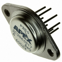
IC PWR AMP 100V 2A 8PIN TO3
Manufacturer
Cirrus Logic Inc
Series
Apex Precision Power™r
Specifications of PB50
Amplifier Type
Power
Number Of Circuits
1
Slew Rate
100 V/µs
-3db Bandwidth
1MHz
Voltage - Input Offset
750mV
Current - Supply
17mA
Current - Output / Channel
2A
Voltage - Supply, Single/dual (±)
60 V ~ 200 V, ±30 V ~ 100 V
Operating Temperature
-25°C ~ 85°C
Mounting Type
Through Hole
Package / Case
TO-3-8
Number Of Channels
1
Input Offset Voltage
0.00175 mV
Maximum Operating Temperature
+ 85 C
Mounting Style
Through Hole
Maximum Dual Supply Voltage
+/- 100 V
Minimum Operating Temperature
- 25 C
For Use With
598-1392 - KIT EVAL PB50/PB58 PWR BOOSTER
Lead Free Status / RoHS Status
Request inventory verification / RoHS compliant by exemption
Output Type
-
Gain Bandwidth Product
-
Current - Input Bias
-
Lead Free Status / Rohs Status
Details
Other names
598-1338
Available stocks
Company
Part Number
Manufacturer
Quantity
Price

Part Number:
PB50
Manufacturer:
APEX
Quantity:
20 000
Part Number:
PB50005
Manufacturer:
ZV
Quantity:
20 000
Part Number:
PB5001
Manufacturer:
ZV
Quantity:
20 000
Part Number:
PB5002
Manufacturer:
ZV
Quantity:
20 000
Part Number:
PB5004
Manufacturer:
ZV
Quantity:
20 000
Company:
Part Number:
PB5008-E3/45
Manufacturer:
PANASONIC
Quantity:
230


PB50
GENERAL
siderations" which covers stability, supplies, heat sinking,
mounting, current limit, SOA interpretation, and specification
interpretation. Visit www.Cirrus.com for design tools that help
automate tasks such as calculations for stability, internal power
dissipation, current limit; heat sink selection; Apex Precision
Power’s complete Application Notes library; Technical Seminar
Workbook; and Evaluation Kits.
CURRENT LIMIT
con nected as shown in the external connection diagram. The
minimum value is 0.27Ω with a maximum practical value of
47Ω. For optimum reliability the resistor value should be set
as high as possible. The value is calculated as follows: +I
.65/R
SAFE OPERATING AREA (SOA)
However, for protection against sustained, high energy flyback,
external fast-recovery diodes should be used.
COMPOSITE AMPLIFIER CONSIDERATIONS
advantages, but also requires careful consideration of several
amplifier and system parameters. The most important of these
are gain, stability, slew rate, and output swing of the driver.
Operating the booster amplifier in higher gains results in a
higher slew rate and lower output swing requirement for the
driver, but makes stability more difficult to achieve.
GAIN SET
above. The composite amplifier’s closed loop gain is determined
by the feedback network, that is: –Rf/Ri (inverting) or 1+Rf/Ri
(non-inverting). The driver amplifier’s “effective gain” is equal
to the composite gain divided by the booster gain.
4
Please read Application Note 1 "General Operating Con-
For proper operation, the current limit resistor (R
NOTE: The output stage is protected against transient flyback.
Cascading two amplifiers within a feedback loop has many
The booster’s closed-loop gain is given by the equation
Example: Inverting configuration (figure 1) with
CL
+ .010, –I
R
Av =
R i = 2K, R f = 60K, R g = 0 :
SUPPLY TO OUTPUT DIFFERENTIAL VOLTAGE V
.1
3
2
1
G
10
= [ (Av-1) • 3.1K] – 6.2K
R
L
G
3.1K
Av (booster) = (6.2K/3.1K) + 1 = 3
Av (composite) = 60K/2K = - 30
Av (driver) = - 30/3 = -10
= .65/R
+ 6.2K
20
30 40 50
CL
+1
.
SOA
100
200
S
— V
CL
O
300
) must be
(V)
L
=
P r o d u c t I n n o v a t i o n F r o m
STABILITY
guidelines:
1. Operate the booster in the lowest practical gain.
2. Operate the driver amplifier in the highest practical effective
3. Keep gain-bandwidth product of the driver lower than the
4. Minimize phase shift within the loop.
from 3 to 10 with total (composite) gain at least a factor of 3
times booster gain. Guideline (3) implies compensating the
driver as required in low composite gain configurations. Phase
shift within the loop (4) is minimized through use of booster
and loop compensation capacitors Cc and Cf when required.
Typical values are 5pF to 33pF.
driver effective gain is unity (ie; total gain = booster gain). For
this situation, Table 1 gives compensation values for optimum
square wave response with the op amp drivers listed.
Table 1:
Typical values for case where op amp effective gain = 1.
Figure 2. Non-inverting composite amplifier.
SLEW RATE
rate of the driver times the booster gain, with a maximum value
equal to the booster slew rate.
OUTPUT SWING
op amp is equal to the maximum output swing from the booster
divided by the booster gain. The Vos of the booster must also
be supplied by the driver, and should be subtracted from the
available swing range of the driver. Note also that effects of Vos
drift and booster gain accuracy should be considered when
calculating maximum available driver swing.
Stability can be maximized by observing the following
A good compromise for (1) and (2) is to set booster gain
Stability is the most difficult to achieve in a configuration where
DRIVER
OP07
741
LF155
LF156
TL070
For: R
The slew rate of the composite amplifier is equal to the slew
The maximum output voltage swing required from the driver
gain.
closed loop bandwidth of the booster.
R
V
F
I
IN
= 33K, R
OP
AMP
C
-
-
-
-
22p
I
+15V
–15V
CH
= 3.3K, R
C
CH
C
COM
F
C
22p
18p
4.7p
4.7p
15p
R
F
F
IN
G
+Vs
= 22K
–Vs
PB50
C
22p
10p
10p
10p
10p
C
GAIN
COMP
R
C
R
CL
C
OUT
G
FPBW
4kHz
20kHz
60kHz
80kHz
80kHz
R
PB50U
L
SR
1.5
7
>60
>60
>60
Related parts for PB50
Image
Part Number
Description
Manufacturer
Datasheet
Request
R

Part Number:
Description:
Development Kit
Manufacturer:
Cirrus Logic Inc
Datasheet:
Part Number:
Description:
Development Kit
Manufacturer:
Cirrus Logic Inc
Datasheet:


Part Number:
Description:
High-efficiency PFC + Fluorescent Lamp Driver Reference Design
Manufacturer:
Cirrus Logic Inc
Datasheet:
Part Number:
Description:
Development Kit
Manufacturer:
Cirrus Logic Inc
Datasheet:
Part Number:
Description:
Development Kit
Manufacturer:
Cirrus Logic Inc
Datasheet:

Part Number:
Description:
Development Kit
Manufacturer:
Cirrus Logic Inc
Datasheet:
Part Number:
Description:
Development Kit
Manufacturer:
Cirrus Logic Inc
Datasheet:
Part Number:
Description:
Development Kit
Manufacturer:
Cirrus Logic Inc
Datasheet:
Part Number:
Description:
Development Kit
Manufacturer:
Cirrus Logic Inc
Datasheet:

Part Number:
Description:
EVALUATION BOARD FOR CS8427
Manufacturer:
Cirrus Logic Inc
Datasheet:

Part Number:
Description:
BOARD EVAL FOR CS8416 RCVR
Manufacturer:
Cirrus Logic Inc
Datasheet:

Part Number:
Description:
EVALUATION BOARD FOR CS8420
Manufacturer:
Cirrus Logic Inc
Datasheet:

Part Number:
Description:
KIT DEVELOPMENT EP9315 ARM9
Manufacturer:
Cirrus Logic Inc
Datasheet:

Part Number:
Description:
KIT DEVELOPMENT EP9302 ARM9
Manufacturer:
Cirrus Logic Inc
Datasheet: