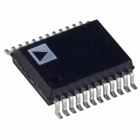
AD604ARSZ Analog Devices Inc, AD604ARSZ Datasheet - Page 22

AD604ARSZ
Manufacturer Part Number
AD604ARSZ
Description
IC AMP VGA DUAL ULN 40MA 24SSOP
Manufacturer
Analog Devices Inc
Series
X-AMP®r
Datasheet
1.AD604-EVALZ.pdf
(32 pages)
Specifications of AD604ARSZ
Amplifier Type
Variable Gain
Number Of Circuits
2
Slew Rate
170 V/µs
-3db Bandwidth
40MHz
Current - Input Bias
400nA
Current - Supply
32mA
Current - Output / Channel
40mA
Operating Temperature
-40°C ~ 85°C
Mounting Type
Surface Mount
Package / Case
24-SSOP
No. Of Amplifiers
1
Bandwidth
40MHz
Gain Accuracy
1.2dB
No. Of Channels
2
Supply Voltage Range
± 5V
Amplifier Case Style
SSOP
No. Of Pins
24
Operating Temperature Range
-40°C To +85°C
Lead Free Status / RoHS Status
Lead free / RoHS Compliant
For Use With
AD604-EVALZ - BOARD EVAL FOR AD604 AMP
Output Type
-
Voltage - Supply, Single/dual (±)
-
Gain Bandwidth Product
-
Voltage - Input Offset
-
Lead Free Status / RoHS Status
Lead free / RoHS Compliant, Lead free / RoHS Compliant
Available stocks
Company
Part Number
Manufacturer
Quantity
Price
Part Number:
AD604ARSZ
Manufacturer:
ADI/亚德诺
Quantity:
20 000
AD604
MEDICAL ULTRASOUND TGC DRIVING THE
AD9050, A 10-BIT, 40 MSPS ADC
The AD604 is an ideal candidate for the time gain control (TGC)
amplifier that is required in medical ultrasound systems to limit
the dynamic range of the signal that is presented to the ADC.
Figure 52 shows a schematic of an AD604 driving an
in a typical medical ultrasound application.
ANALOG
INPUT
J2
0.1µF
0.1µF
VREF
50Ω
0.1µF
50Ω
0.1µF
DIGITAL GAIN CONTROL
10
11
12
10
1
2
3
4
5
6
7
8
9
1
2
3
4
5
6
7
8
9
–DSX1
+DSX1
PAO1
FBK1
PAI1
COM1
COM2
PAI2
FBK2
PAO2
+DSX2
–DSX2
V
V
V
V
AGND
DGND
DB7
(MSB)
DB6
DB5
DB4
OUT
OUT
SS
REF
AD7226
AD604
B
A
100Ω
V
V
VOCM
VNEG
VNEG
VGN1
GND1
VPOS
VPOS
GND2
VGN2
VREF
OUT1
OUT2
(LSB)
OUT
OUT
DB0
DB1
DB2
DB3
V
WR
A0
A1
DD
Figure 52. TGC Circuit for Medical Ultrasound Application
C
D
20
19
18
17
16
15
14
13
12
11
24
23
22
21
20
19
18
17
16
15
14
13
0.1µF
1kΩ
AD9050
0.1µF
+15V
FILTER
0.1µF
0.1µF
Rev. G | Page 22 of 32
+5V
–5V
1kΩ
2
3
The gain is controlled by means of a digital byte that is input to
an
The output common-mode voltage of the AD604 is set to VPOS/2
by means of an internal voltage divider. The VOCM pin is
bypassed with a 0.1 μF capacitor to ground.
The DSX output is optionally filtered and then buffered by
an
op amp output is ac-coupled into the self-biasing input of an
AD9050
sampling rate.
–IN
+IN
AD7226
AD9631
OPTIONAL
1kΩ
AD9631
OUT
ADC that is capable of outputting 10 bits at a 40 MSPS
0.1µF
6
op amp, a low distortion, low noise amplifier. The
DAC that outputs the analog gain control signal.
0.1µF
0.1µF
0.1µF
10
13
14
3
4
5
6
9
AIN
VREF
VREF
COMP
REF
AINB
ENCODE
OR
AD9050
BP
OUT
IN
(MSB) D9
(LSB) D0
V
V
D8
D7
D6
D5
D4
D3
D2
D1
DD
DD
15
16
17
18
19
24
25
26
27
28
20
22
CLK
A/D
OUTPUT


