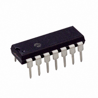
TC7650CPD Microchip Technology, TC7650CPD Datasheet - Page 2

TC7650CPD
Manufacturer Part Number
TC7650CPD
Description
IC OPAMP CHOPPER STAB 14DIP
Manufacturer
Microchip Technology
Datasheet
1.TC7650CPA.pdf
(14 pages)
Specifications of TC7650CPD
Slew Rate
2.5 V/µs
Amplifier Type
Chopper (Zero-Drift)
Number Of Circuits
1
Gain Bandwidth Product
2MHz
Current - Input Bias
1.5pA
Voltage - Input Offset
0.7µV
Current - Supply
2mA
Voltage - Supply, Single/dual (±)
4.5 V ~ 16 V, ±2.25 V ~ 8 V
Operating Temperature
0°C ~ 70°C
Mounting Type
Through Hole
Package / Case
14-DIP (0.300", 7.62mm)
Op Amp Type
Chopper Stabilized
No. Of Amplifiers
1
Bandwidth
2MHz
Supply Voltage Range
4.5V To 16V
Amplifier Case Style
DIP
No. Of Pins
14
Number Of Channels
1
Voltage Gain Db
130 dB
Common Mode Rejection Ratio (min)
120 dB
Input Offset Voltage
0.001 mV
Supply Current
3.5 mA
Maximum Power Dissipation
730 mW
Maximum Operating Temperature
+ 70 C
Mounting Style
Through Hole
Maximum Dual Supply Voltage
+/- 8 V
Minimum Operating Temperature
0 C
Lead Free Status / RoHS Status
Lead free / RoHS Compliant
Output Type
-
Current - Output / Channel
-
-3db Bandwidth
-
Lead Free Status / Rohs Status
Details
Available stocks
Company
Part Number
Manufacturer
Quantity
Price
Company:
Part Number:
TC7650CPD
Manufacturer:
XR
Quantity:
6 273
TC7650
General Description
The TC7650 CMOS chopper stabilized operational
amplifier practically removes offset voltage error terms
from system error calculations. The 5µV maximum V
specification, for example, represents a 15 times
improvement over the industry standard OP07E. The
50nV/°C offset drift specification is over 25 times lower
than the OP07E. The increased performance elimi-
nates V
adjustment and the reliability problems caused by dam-
aged trimmers.
The TC7650 performance advantages are achieved
without the additional manufacturing complexity and
cost incurred with laser or "zener zap" V
niques.
Functional Block Diagram
DS21463B-page 2
OS
trim procedures, periodic potentiometer
Inputs
Output
Clamp
*
For 8-Pin DIP, connect to V ss
A
B
Output Clamp
NULL
Null
Main
Amplifier
Circuit
Null
Amplifier
OS
B
Compensation
trim tech-
Intermod
OS
The TC7650 nulling scheme corrects both DC V
errors and V
amplifier alternately corrects its own V
main amplifier V
stored on two user supplied external capacitors. The
capacitors connect to the internal amplifier V
points. The main amplifier input signal is never
switched. Switching spikes are not present at the
TC7650 output.
The 14-pin dual-in-line package (DIP) has an external
oscillator input to drive the nulling circuitry for optimum
noise performance. Both the 8 and 14-pin DIPs have
an output voltage clamp circuit to minimize overload
recovery time.
B
Oscillator
A
A
B
OS
drift errors with temperature. A nulling
*C
OS
TC7650
RETN
C
C
14-Pin DIP Only
B
A
error. Offset nulling voltages are
INT/EXT
EXT CLK IN
CLK OUT
©
2002 Microchip Technology Inc.
Output
OS
errors and the
OS
null
OS


