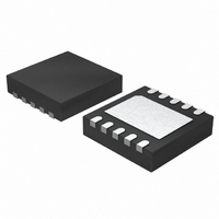
LT1995CDD#PBF Linear Technology, LT1995CDD#PBF Datasheet - Page 15

LT1995CDD#PBF
Manufacturer Part Number
LT1995CDD#PBF
Description
IC AMP GAIN SELECT 10-DFN
Manufacturer
Linear Technology
Datasheet
1.LT1995CMSPBF.pdf
(20 pages)
Specifications of LT1995CDD#PBF
Amplifier Type
Programmable Gain
Number Of Circuits
1
Slew Rate
1000 V/µs
-3db Bandwidth
32MHz
Voltage - Input Offset
750µV
Current - Supply
7.1mA
Current - Output / Channel
120mA
Voltage - Supply, Single/dual (±)
5 V ~ 30 V, ±2.5 V ~ 15 V
Operating Temperature
0°C ~ 70°C
Mounting Type
Surface Mount
Package / Case
10-WFDFN Exposed Pad
Lead Free Status / RoHS Status
Lead free / RoHS Compliant
Output Type
-
Gain Bandwidth Product
-
Current - Input Bias
-
Available stocks
Company
Part Number
Manufacturer
Quantity
Price
APPLICATIO S I FOR ATIO
AC-Coupling Methods for Single Supply Operation
The LT1995 can be used in many single-supply applications
using AC-coupling without additional biasing circuitry.
AC-coupling the LT1995 in a difference amplifier configu-
ration (as in Figure 1) is a simple matter of adding coupling
capacitors to each input and the output as shown in the
example of Figure 5. The input voltage V
REF pin establishes the quiescent voltage on the input and
output pins. The V
impedance to avoid degrading the CMRR (0.5Ω for
1dB CMRR change typically).
V
V
V
IN
IN
IN
*
*
*
10
10
10
8
9
1
2
3
8
9
1
2
3
8
9
1
2
3
BIAS
U
*CONFIGURE M INPUTS FOR DESIRED G PARAMETER; REFER TO FIGURE 2 FOR CONNECTIONS
M4
M2
M1
P1
P2
P4
M4
M2
M1
P1
P2
P4
M4
M2
M1
P1
P2
P4
LT1995
LT1995
LT1995
signal should have a low source
A = 0.875
A = 0.800
A = 0.667
–V
–V
–V
U
4
4
4
+V
+V
+V
Figure 3. Noninverting Amplifier Input Attenuation Configurations (A > 0.5)
7
7
7
REF
REF
REF
5
5
5
W
6
6
6
V
V
V
OUT
OUT
OUT
BIAS
V
IN
applied to the
V
V
IN
IN
*
*
*
U
10
10
10
8
9
1
2
3
8
9
1
2
3
8
9
1
2
3
M4
M2
M1
P1
P2
P4
M4
M2
M1
P1
P2
P4
M4
M2
M1
P1
P2
P4
LT1995
LT1995
LT1995
A = 0.857
A = 0.750
A = 0.625
–V
–V
–V
4
4
4
+V
+V
+V
7
7
7
REF
REF
REF
5
5
5
6
6
6
Figure 4. Unique Noninverting Gain Configurations
V
V
V
OUT
OUT
OUT
8
7
5
3
1
6
4
2
1
V
V
V
IN
IN
IN
*
*
*
10
10
10
GAIN COMBINATION
8
9
1
2
3
8
9
1
2
3
8
9
1
2
3
M4
M2
M1
P1
P2
P4
M4
M2
M1
P1
P2
P4
M4
M2
M1
P1
P2
P4
LT1995
LT1995
LT1995
A = 0.833
A = 0.714
A = 0.571
–V
–V
–V
4
4
4
+V
+V
+V
7
7
7
REF
REF
REF
5
5
5
6
6
6
1995 F04
1995 F03
V
V
V
73
OUT
OUT
OUT
LT1995
15
1995fb


