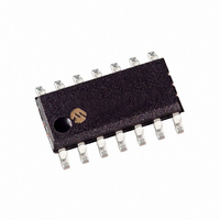
MCP6274-E/SL Microchip Technology, MCP6274-E/SL Datasheet - Page 2

MCP6274-E/SL
Manufacturer Part Number
MCP6274-E/SL
Description
IC OPAMP 2.0V QUAD R-R 14SOIC
Manufacturer
Microchip Technology
Specifications of MCP6274-E/SL
Slew Rate
0.9 V/µs
Package / Case
14-SOIC (3.9mm Width), 14-SOL
Amplifier Type
General Purpose
Number Of Circuits
4
Output Type
Rail-to-Rail
Gain Bandwidth Product
2MHz
Current - Input Bias
1pA
Voltage - Input Offset
3000µV
Current - Supply
170µA
Current - Output / Channel
25mA
Voltage - Supply, Single/dual (±)
2 V ~ 6 V
Operating Temperature
-40°C ~ 125°C
Mounting Type
Surface Mount
Number Of Channels
4
Common Mode Rejection Ratio (min)
70 dB
Input Offset Voltage
3 mV
Input Bias Current (max)
1 pA
Operating Supply Voltage
3 V, 5 V
Maximum Operating Temperature
+ 125 C
Minimum Operating Temperature
- 40 C
Mounting Style
SMD/SMT
Shutdown
No
Supply Voltage (max)
5.5 V
Supply Voltage (min)
2 V
Technology
CMOS
Voltage Gain Db
110 dB
Lead Free Status / RoHS Status
Lead free / RoHS Compliant
-3db Bandwidth
-
Lead Free Status / Rohs Status
Lead free / RoHS Compliant
Available stocks
Company
Part Number
Manufacturer
Quantity
Price
Company:
Part Number:
MCP6274-E/SL
Manufacturer:
MURATA
Quantity:
1 200
Part Number:
MCP6274-E/SL
Manufacturer:
MICROCHIP/微芯
Quantity:
20 000
Part Number:
MCP6274-E/SL/SOL342108
Manufacturer:
MICROCHIP/微芯
Quantity:
20 000
MCP6271/1R/2/3/4/5
1.0
Absolute Maximum Ratings †
V
Current at Input Pins ....................................................±2 mA
Analog Inputs (V
All other Inputs and Outputs .......... V
Difference Input Voltage ...................................... |V
Output Short Circuit Current .................................Continuous
Current at Output and Supply Pins ............................±30 mA
Storage Temperature....................................–65°C to +150°C
Junction Temperature (T
ESD Protection On All Pins (HBM/MM) ................ ≥ 4 kV/400V
DC ELECTRICAL SPECIFICATIONS
DS21810F-page 2
Electrical Characteristics: Unless otherwise indicated, T
V
Input Offset (Note 1)
Input Offset Voltage
Input Offset Voltage
Input Offset Temperature Drift
Power Supply Rejection Ratio
Input Bias Current and Impedance
Input Bias Current
Input Offset Current
Common Mode Input Impedance
Differential Input Impedance
Common Mode (Note 4)
Common Mode Input Voltage Range
Common Mode Rejection Ratio
Common Mode Rejection Ratio
Open-Loop Gain
DC Open-Loop Gain (Large Signal)
Note 1:
DD
OUT
(Extended Temperature)
– V
At Temperature
At Temperature
≈ V
2:
3:
4:
5:
6:
7:
SS
ELECTRICAL
CHARACTERISTICS
DD
........................................................................7.0V
/2, V
Parameters
The MCP6275’s V
The current at the MCP6275’s V
This specification does not apply to the MCP6275’s V
The MCP6275’s V
V
has a voltage range specified by V
Set by design and characterization.
Does not apply to op amp B of the MCP6275.
All parts with date codes November 2007 and later have been screened to ensure operation at V
the other minimum and maximum specifications are measured at 2.0V and 5.5V.
DD
IN
L
– 100 mV. CMRR is not measured for op amp B of the MCP6275. The MCP6275’s V
+ and V
= V
DD
J
/2, R
) . .........................................+150°C
IN
–) †† .. V
L
CM
= 10 kΩ to V
INB
– pin (op amp B) has a common mode input voltage range (V
for op amp B (pins V
SS
SS
ΔV
– 1.0V to V
– 0.3V to V
CMRR
CMRR
PSRR
V
V
Z
Sym
V
V
OS
Z
A
I
DIFF
CMR
CMR
I
I
I
OS
CM
OS
OS
OL
L
B
B
B
/ΔT
INB
and CS is tied low. (Refer to
OH
A
– pin is specified by I
DD
DD
V
V
and V
DD
SS
SS
+ 1.0V
+ 0.3V
–3.0
–5.0
– V
Min
70
70
65
90
OUTA
—
—
—
—
—
—
—
− 0.15
− 0.30
OL
SS
A
.
= +25°C, V
/V
|
INB
+ and V
10
10
OUTA
±1.7
±1.0
±1.0
Typ
110
90
50
85
80
—
—
13
13
—
—
2
B
||6
||3
only.
† Notice: Stresses above those listed under “Absolute
Maximum Ratings” may cause permanent damage to the
device. This is a stress rating only and functional operation of
the device at those or any other conditions above those
indicated in the operational listings of this specification is not
implied. Exposure to maximum rating conditions for extended
periods may affect device reliability.
†† See Section 4.1.2 “Input Voltage and Current Limits”.
/V
DD
INB
INB
Figure 1-2
= +2.0V to +5.5V, V
–) is V
V
V
+ pin.
DD
DD
+3.0
+5.0
Max
200
—
—
—
—
—
—
—
—
—
+ 0.15
+ 0.30
5
SS
and
+ 100 mV.
µV/°C T
Figure
Units
Ω||pF Note 3
Ω||pF Note 3
mV
mV
dB
pA
pA
nA
pA
dB
dB
dB
V
V
SS
CMR
1-3).
= GND, V
V
T
V
Note 2
T
T
Note 3
V
V
V
(Note 6)
V
(Note 6)
V
V
© 2008 Microchip Technology Inc.
A
A
A
A
CM
CM
DD
DD
CM
CM
OUT
CM
= +85°C (Note 2)
= +125°C (Note 2)
= –40°C to +125°C, V
= –40°C to +125°C, V
) of V
= 2.0V (Note 5)
= 5.5V (Note 5)
= –0.3V to 2.5V, V
= –0.3V to 5.3V, V
= V
= V
= V
OUTA
= 0.2V to V
SS
SS
SS
SS
CM
/V
Conditions
(Note 1)
+ 100 mV to
DD
INB
= V
= 6.0V. However,
+ pin (op amp B)
DD
DD
/2,
– 0.2V,
DD
DD
CM
CM
= 5V
= 5V
= V
= V
SS
SS


