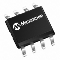
MCP6G03-E/MS Microchip Technology, MCP6G03-E/MS Datasheet - Page 20

MCP6G03-E/MS
Manufacturer Part Number
MCP6G03-E/MS
Description
IC GAIN BLOCK 1.8V 1CH 8MSOP
Manufacturer
Microchip Technology
Datasheet
1.MCP6G01UT-EOT.pdf
(38 pages)
Specifications of MCP6G03-E/MS
Amplifier Type
General Purpose
Number Of Circuits
1
Output Type
Rail-to-Rail
Slew Rate
4.5 V/µs
-3db Bandwidth
900kHz
Current - Input Bias
1pA
Voltage - Input Offset
1000µV
Current - Supply
110µA
Current - Output / Channel
20mA
Voltage - Supply, Single/dual (±)
1.8 V ~ 5.5 V
Operating Temperature
-40°C ~ 125°C
Mounting Type
Surface Mount
Package / Case
8-MSOP, Micro8™, 8-uMAX, 8-uSOP,
No. Of Amplifiers
1
Bandwidth
900kHz
No. Of Channels
1
Supply Voltage Range
1.8V To 5.5V
Amplifier Case Style
MSOP
No. Of Pins
8
Operating Temperature Range
-40°C To +125°C
Rohs Compliant
Yes
Lead Free Status / RoHS Status
Lead free / RoHS Compliant
Gain Bandwidth Product
-
Available stocks
Company
Part Number
Manufacturer
Quantity
Price
Company:
Part Number:
MCP6G03-E/MS
Manufacturer:
MICROCHIP
Quantity:
12 000
MCP6G01/1R/1U/2/3/4
4.1.4
The ESD protection on the inputs can be depicted as
shown in
protect the input transistors, and to minimize input bias
current (I
when they try to go more than one diode drop below
V
above V
allow normal operation, and low enough to bypass ESD
events within the specified limits.
FIGURE 4-2:
Structures.
In order to prevent damage and/or improper operation
of these amplifiers, the circuits they are in must limit the
currents (and voltages) at the V
“Absolute Maximum Ratings †” at the beginning of
Section 1.0 “Electrical Characteristics”).
shows the recommended approach to protecting these
inputs. The internal ESD diodes prevent the input pins
(V
R
Diode D
above V
also limits the current through D
FIGURE 4-3:
Inputs.
It is also possible to connect the diode to the left of the
resistor R
D
resistor then serves as in-rush current limiter; the DC
DS22004B-page 20
SS
1
1
IN
limits the possible current drawn out of the input pin.
needs to be limited by some other mechanism. The
. They also clamp any voltages that go too far
) from going too far below ground, and the resistor
V
V
V
DD
SS
V
IN
1
1
DD
DD
B
R
prevents the input pin (V
1
). The input ESD diodes clamp the inputs
. In this case, the current through the diode
Figure
Bond
Bond
Bond
; their breakdown voltage is high enough to
. When implemented as shown, resistor R
1
Pad
Pad
Pad
INPUT VOLTAGE AND CURRENT
LIMITS
≥
R
V
1
SS
D
4-2. This structure was chosen to
1
– (minimum expected V
V
IN
Simplified Analog Input ESD
Protecting the Analog
Stage
Input
MCP6G0X
2 mA
V
DD
1
.
IN
IN
) from going too far
pins (see Section
to the rest of
the amplifier
V
1
Figure 4-3
OUT
)
1
current into the input pin (V
A significant amount of current can flow out of the
inputs when the common mode voltage (V
ground (V
high impedance may need to limit the useable voltage
range.
4.1.5
The maximum output voltage swing is the maximum
swing possible under a particular amplifier load current.
The amplifier load current is the sum of the external
load current (I
resistance (I
EQUATION 4-2:
FIGURE 4-4:
See
(V
load current.The specification table states the output
can reach within 10 mV of either supply rail when
R
4.2
The
(R
switches in series with the inverting input reduces the
parasitic capacitance, distortion, and gain mismatch.
R
causes additional current draw from the supplies.
When CS is high, the SGA is shut down (low power).
R
these pins and the internal amplifier’s inverting input
are all connected through R
high-Z (unlike the internal op amp).
R
LAD
LAD
LAD
L
DD
LAD
= 100 kΩ.
Figure 2-20
is an additional load on the output of the SGA and
– V
is still attached to the V
contributes to the output noise; see
= R
resistor
Where:
V
Resistor Ladder
IN
OH
Amplifier Load Current
F
SS
RAIL-TO-RAIL OUTPUT
+ R
LAD
); see
or V
OUT
MCP6G0X
G
); see
) sets the gain. Placing the gain
OL
I
) and the current through the ladder
LAD
ladder
for the typical output headroom
Figure
– V
Figure
Amplifier Load Current.
=
© 2006 Microchip Technology Inc.
SS
(
-------------------------------- -
) as a function of amplifier
2-17. Applications that are
V
IN
OUT
shown
LAD
) should be very small.
4-4.
V
OUT
R
SS
LAD
=
–
I
R
and the output is not
OUT
I
and V
V
LAD
LAD
I
OUT
SS
)
in
SS
+
V
Figure
CM
I
OUT
LAD
pins. Thus,
Figure 4-1
) is below
2-9.


