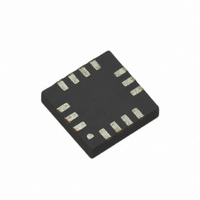
LMH6554LEE/NOPB National Semiconductor, LMH6554LEE/NOPB Datasheet - Page 4

LMH6554LEE/NOPB
Manufacturer Part Number
LMH6554LEE/NOPB
Description
IC OP AMP DIFF 2.8GHZ 14LLP
Manufacturer
National Semiconductor
Series
PowerWise®r
Datasheet
1.LMH6554LEENOPB.pdf
(16 pages)
Specifications of LMH6554LEE/NOPB
Amplifier Type
Differential
Number Of Circuits
1
Output Type
Differential
Slew Rate
6200 V/µs
-3db Bandwidth
2.8GHz
Current - Input Bias
1µA
Voltage - Input Offset
6500µV
Current - Supply
52mA
Current - Output / Channel
150mA
Voltage - Supply, Single/dual (±)
4.7 V ~ 5.25 V
Operating Temperature
-40°C ~ 125°C
Mounting Type
Surface Mount
Package / Case
14-LLP
No. Of Amplifiers
1
Input Offset Voltage
3mV
Bandwidth
2.8GHz
Supply Voltage Range
4.7V To 5.25V
Supply Current
52mA
Amplifier Case Style
LLP
No. Of Pins
14
Rohs Compliant
Yes
Lead Free Status / RoHS Status
Lead free / RoHS Compliant
Gain Bandwidth Product
-
Other names
LMH6554LEETR
Note 1: Absolute Maximum Ratings indicate limits beyond which damage to the device may occur. Operating Ratings indicate conditions for which the device is
intended to be functional, but specific performance is not guaranteed. For guaranteed specifications, see the Electrical Characteristics tables.
Note 2: Electrical Table values apply only for factory testing conditions at the temperature indicated. Factory testing conditions result in very limited self-heating
of the device such that T
= T
. No guarantee of parametric performance is indicated in the electrical tables under conditions of internal self-heating where
J
A
T
> T
. See Applications Section for information on temperature de-rating of this device." Min/Max ratings are based on product characterization and simulation.
J
A
Individual parameters are tested as noted.
, θ
Note 3: The maximum power dissipation is a function of T
. The maximum allowable power dissipation at any ambient temperature is
J(MAX)
JA
) / θ
P
= (T
– T
. All numbers apply for packages soldered directly onto a PC Board.
D
J(MAX)
A
JA
Note 4: The maximum output current (I
) is determined by device power dissipation limitations. See the Power Dissipation section of the Application Section
OUT
for more details.
Note 5: Human Body Model, applicable std. MIL-STD-883, Method 30157. Machine Model, applicable std. JESD22-A115-A (ESD MM std. of JEDEC). Field-
Induced Charge-Device Model, applicable std. JESD22-C101-C (ESD FICDM std. of JEDEC).
Note 6: Short circuit current should be limited in duration to no more than 10 seconds. See the Power Dissipation section of the Application Information for more
details.
Note 7: Typical values represent the most likely parametric norm as determined at the time of characterization. Actual typical values may vary over time and will
also depend on the application and configuration. The typical values are not tested and are not guaranteed on shipped production material.
Note 8: Limits are 100% production tested at 25°C. Limits over the operating temperature range are guaranteed through correlation using Statistical Quality
Control (SQC) methods.
Note 9: Negative input current implies current flowing out of the device.
Note 10: I
is referred to a differential output offset voltage by the following relationship: V
= I
*2R
BI
OD(OFFSET)
BI
F
www.national.com
4


