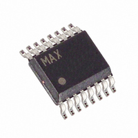
MAX4022EEE+ Maxim Integrated Products, MAX4022EEE+ Datasheet - Page 3

MAX4022EEE+
Manufacturer Part Number
MAX4022EEE+
Description
IC BUFFER R-R 16-QSOP
Manufacturer
Maxim Integrated Products
Datasheet
1.MAX4019ESD.pdf
(12 pages)
Specifications of MAX4022EEE+
Amplifier Type
Buffer
Number Of Circuits
4
Output Type
Rail-to-Rail
Slew Rate
600 V/µs
-3db Bandwidth
200MHz
Current - Input Bias
5.4µA
Voltage - Input Offset
4000µV
Current - Supply
5.5mA
Current - Output / Channel
120mA
Voltage - Supply, Single/dual (±)
3.15 V ~ 11 V, ±1.575 V ~ 5.5 V
Operating Temperature
-40°C ~ 85°C
Mounting Type
Surface Mount
Package / Case
16-QSOP
Number Of Channels
4
Voltage Gain Db
6.02 dB
Input Offset Voltage
4 mV
Operating Supply Voltage
5 V, 9 V
Maximum Power Dissipation
667 mW
Maximum Operating Temperature
+ 85 C
Mounting Style
SMD/SMT
Maximum Dual Supply Voltage
+/- 5.5 V
Minimum Operating Temperature
- 40 C
Lead Free Status / RoHS Status
Lead free / RoHS Compliant
Gain Bandwidth Product
-
Lead Free Status / Rohs Status
Details
AC ELECTRICAL CHARACTERISTICS
(V
otherwise noted. Typical values are at T
Note 1: The MAX4014EUK is 100% production tested at T
Note 2: Tested with V
Note 3: PSRR for single +5V supply tested with V
Note 4: Guaranteed by design.
Small-Signal -3dB Bandwidth
Large-Signal -3dB Bandwidth
Bandwidth for 0.1dB Gain
Flatness
Slew Rate
Settling Time to 0.1%
Rise/Fall Time
Spurious-Free Dynamic
Range
Harmonic Distortion
Third-Order Intercept
Input 1dB Compression Point
Differential Phase Error
Differential Gain Error
Input Noise Voltage Density
Input Noise Current Density
Input Capacitance
Disabled Output Capacitance
Output Impedance
Buffer Enable Time
Buffer Disable Time
Buffer Gain Matching
Buffer Crosstalk
CC
Low-Cost, High-Speed, Single-Supply, Gain of +2
= +5V, V
PARAMETER
design.
V
CC
= +4.5V to +5.5V; and for single +3V supply with V
EE
Buffers with Rail-to-Rail Outputs in SOT23
= 0V, IN_- = 0V, EN_ = 5V, R
_______________________________________________________________________________________
OUT
= +2.5V.
C
SYMBOL
BW
OUT(OFF)
X
BW
BW
SFDR
Z
t
t
R
C
t
HD
IP3
DG
TALK
SR
DP
OFF
OUT
e
ON
0.1dB
t
i
, t
n
S
IN
n
SS
LS
A
F
= +25°C.)
V
V
V
V
V
V
f
V
f
f = 10.0MHz
f
NTSC, R
NTSC, R
f = 10kHz
f = 10kHz
MAX4019, EN_ = 0V
f = 10MHz
MAX4019
MAX4019
MAX4017/MAX4019/MAX4022,
f = 10MHz, V
MAX4017/MAX4019/MAX4022,
f = 10MHz, V
C
C
C
OUT
OUT
OUT
OUT
OUT
OUT
OUT
= 5MHz, V
= 5MHz
= 10MHz, A
EE
L
= 0V, V
= 20mVp-p
= 2Vp-p
= 20mVp-p (Note 4)
= 2V step
= 2V step
= 100mVp-p
= 2Vp-p,
= 100Ω to ground, noninverting configuration, T
L
L
= 150Ω
= 150Ω
A
CC
OUT
OUT
OUT
= +25°C. Specifications over temperature limits are guaranteed by
VCL
CONDITIONS
= +4.5V to +5.5V; for dual ±5V supply with V
EE
= 20mVp-p
= 2Vp-p
= 2Vp-p
= +2V/V
= 0V, V
Second harmonic
Third harmonic
Total harmonic
distortion
CC
= +3.15V to +3.45V.
MIN
6
A
TYP
0.02
0.04
200
140
600
100
-78
-78
-82
-75
-95
1.3
0.1
= T
30
45
35
11
10
EE
1
1
2
6
1
= -4.5V to -5.5V,
MIN
MAX
to T
MAX,
degrees
pA/√Hz
nV/√Hz
UNITS
dBm
dBm
MHz
MHz
MHz
V/µs
dBc
dBc
unless
dB
dB
pF
pF
ns
ns
ns
µs
%
Ω
3


