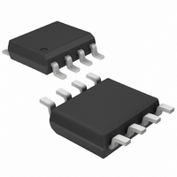
MAX4416ESA+ Maxim Integrated Products, MAX4416ESA+ Datasheet - Page 2

MAX4416ESA+
Manufacturer Part Number
MAX4416ESA+
Description
IC OPAMP DUAL +3/5V R-R 8-SOIC
Manufacturer
Maxim Integrated Products
Datasheet
1.MAX4415ESA.pdf
(22 pages)
Specifications of MAX4416ESA+
Amplifier Type
Voltage Feedback
Number Of Circuits
2
Output Type
Rail-to-Rail
Slew Rate
200 V/µs
-3db Bandwidth
400MHz
Current - Input Bias
1.3µA
Voltage - Input Offset
500µV
Current - Supply
1.6mA
Current - Output / Channel
75mA
Voltage - Supply, Single/dual (±)
2.7 V ~ 5.5 V
Operating Temperature
-40°C ~ 85°C
Mounting Type
Surface Mount
Package / Case
8-SOIC (3.9mm Width)
Number Of Channels
2
Voltage Gain Db
93 dB
Common Mode Rejection Ratio (min)
65 dB
Input Offset Voltage
0.5 mV
Operating Supply Voltage
3 V, 5 V
Maximum Power Dissipation
471 mW
Maximum Operating Temperature
+ 85 C
Mounting Style
SMD/SMT
Minimum Operating Temperature
- 40 C
Lead Free Status / RoHS Status
Lead free / RoHS Compliant
Gain Bandwidth Product
-
Lead Free Status / Rohs Status
Details
ABSOLUTE MAXIMUM RATINGS
Supply Voltage (V
Differential Input Voltage ....................................................±2.5V
IN_-, IN_+, OUT_..............................(V
Current into Input Pins ......................................................±20mA
Output Short-Circuit Duration to V
Continuous Power Dissipation (T
Low-Power, +3V/+5V, 400MHz Single-Supply
Op Amps with Rail-to-Rail Outputs
Stresses beyond those listed under “Absolute Maximum Ratings” may cause permanent damage to the device. These are stress ratings only, and functional
operation of the device at these or any other conditions beyond those indicated in the operational sections of the specifications is not implied. Exposure to
absolute maximum rating conditions for extended periods may affect device reliability.
DC ELECTRICAL CHARACTERISTICS
(V
Typical values are at T
2
Operating Supply Voltage Range
Quiescent Supply Current
(per Amplifier)
Input Common-Mode Voltage
Range
Input Offset Voltage
Input Offset Voltage Temperature
Input Offset Voltage Matching
Input Bias Current
Input Offset Current
Input Resistance
Common-Mode Rejection Ratio
Open-Loop Gain
CC
8-Pin µMAX (derate 4.5mW/°C above +70°C) .............362mW
8-Pin SO (derate 5.9mW/°C above +70°C)..................471mW
14-Pin TSSOP (derate 9.1mW/°C above +70°C) .........727mW
_______________________________________________________________________________________
= +2.7V to +5.5V, V
PARAMETER
CC
to V
A
= +25°C.) (Note 1)
EE
CM
)..................................................+6V
= V
A
CC
CC
= +70°C)
/2 - 0.75V, V
or V
SYMBOL
CC
TC
CMRR
A
V
V
I
R
V
VOL
EE
I
I
OS
CM
OS
VOS
+ 0.3V) to (V
S
B
IN
S
..............Continuous
EE
Guaranteed by PSRR test
Guaranteed by CMRR test
MAX4416–MAX4419
Differential mode,
-0.04V ≤ (V
Common mode,
V
V
V
V
C C
C C
EE
EE
= 0, R
- 0.1V < V
- 0.1V < V
= + 5V
= + 3V
EE
- 0.3V)
L
= ∞ to V
IN+
+0.2V ≤ V
+0.4V ≤ V
+0.3V ≤ V
R
+1V ≤ V
+0.2V ≤ V
+ 0.25V ≤ V
+0.2V ≤ V
R
+0.5V ≤ V
L
L
CM
CM
- V
= 1kΩ to V
= 1kΩ to V
CONDITIONS
IN-
< V
< V
V
V
CC
CC
CC
) ≤ +0.04V
OUT
Operating Temperature Range ...........................-40°C to +85°C
Junction Temperature ......................................................+150°C
Storage Temperature Range .............................-65°C to +150°C
Lead Temperature (soldering, 10s) .................................+300°C
CC
CC
/2, V
OUT
OUT
OUT
OUT
OUT
OUT
OU T
= +5V
= +3V
- 1.5V
- 1.5V
≤ +4V, R
EE
EE
≤ +4.8V, R
≤ +4.6V, R
≤ +4.4V,
≤ +2.8V, R
≤ +2.5V,
≤ +2.5V, R
OUT
≤ + 2.75V , R
= V
L
CC
= 150Ω
L
L
L
L
/2, T
L
= 10kΩ
= 1kΩ
= 10kΩ
= 150Ω
= 1kΩ
A
= T
MIN
V
MIN
0.1
2.7
EE
65
78
68
66
75
65
63
to T
-
MAX
TYP
, unless otherwise noted.
1.6
1.4
0.5
1.3
0.1
±1
60
16
94
93
80
80
65
90
78
75
62
3
V
MAX
5.5
2.6
1.5
0.7
CC
3
6
4
-
UNITS
µV/°C
MΩ
mA
mV
mV
µA
µA
kΩ
dB
dB
V
V


