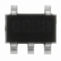
NJM2711F-TE1# NJR, NJM2711F-TE1# Datasheet

NJM2711F-TE1#
Specifications of NJM2711F-TE1#
NJM#2711F-TE1TR
NJM#2711F-TE1TR
NJM2711F-TE1#TR
Related parts for NJM2711F-TE1#
NJM2711F-TE1# Summary of contents
Page 1
... Package Outline PIN CONFIGURATION NJM2711F (Top View) OUT +INPUT 4 ( 2.0 to 4.5V (1.9mA typ 2.5V) (260V/ s typ.) (1GHz typ.) (10MHz typ. at 40dB) (180MHz typ.) (7mV max.) ( 1.5V typ = (75dB typ.) MTP5 + V INPUT - NJM2711 PACKAGR OUTLINE NJM2711F PIN FUNCTION 1.OUTPUT - 2.V 3.+INPUT 4.-INPUT + ...
Page 2
NJM2711 ABSOLUTE MAXIMUM RATINGS PARAMETER Supply Voltage Differential Input Voltage Power Dissipation Operating Temperature Range Storage Temperature Range RECOMMENDED OPERATING CONDITION PARAMETER Operating Voltage Range DC CHARACTERISTICS PARAMETER Operating Current Input Offset Voltage Input Bias Current Input Offset Current Open ...
Page 3
Note: non-inverting amplifier 1.The closed gain should be 6dB or higher to prevent the oscillation. Unity gain follower application may cause the oscillation. 2.When the closed gain is lower than 20dB, use a compensation capacitor (CF: about 5pF), parallel with ...
Page 4
NJM2711 TYPICAL CHARACTERISTICS Operating Current vs.Operating Voltage Vin=0V,Ta=25°C 2.5 2 1.5 1 0.5 0 ±0 ±1 ± Operating Voltage [V] Input Offset Voltage vs. Ambient Temperature + - V /V =±2.5V 0.5 0 -0.5 -1 -1.5 ...
Page 5
Maximum Output Voltage Swing vs. Ambient Temperature + - V /V =±2.5V 2 1.5 1 0.5 0 -0.5 -1 -1 100 Ambient Temperature [°C] Common Mode Rejection Ratio vs. Ambient Temperature + - V /V =±2.5V,-1V<Vcm<+1V ...
Page 6
NJM2711 Pulse Responce + - V /V =±2.5V,f=5MHz,V =2VPP =1kΩ,C =5pF,R =1kΩ,R =2kΩ, 1.0 0.0 -1.0 -2.0 -3.0 -4.0 -5.0 0.0 0.0 0.1 0.1 0.1 Time [10ns/div] Pulse Response (correlation with RL) + ...
Page 7
Voltage Gain vs. Frequency (correlation with RL =±2.5V,V =0.02Vpp,G =40dB,R =50Ω =1.98kΩ,R =20Ω,C =5pF,C =10pF,Ta=+25℃ RL=open 40 Gain 30 RL=2kΩ Phase -10 -20 -30 ...
Page 8
NJM2711 MEASUREMENT CIRCUIT - 8 - DUT [CAUTION] The specifications on this databook are only given for information , without any guarantee as regards either mistakes or omissions. The application circuits in this databook are ...


