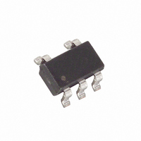
MAX4250EUK+T Maxim Integrated Products, MAX4250EUK+T Datasheet - Page 10

MAX4250EUK+T
Manufacturer Part Number
MAX4250EUK+T
Description
IC OP AMP R-R LN SOT23-5
Manufacturer
Maxim Integrated Products
Datasheet
1.MAX4252EBLT.pdf
(19 pages)
Specifications of MAX4250EUK+T
Amplifier Type
General Purpose
Number Of Circuits
1
Output Type
Push-Pull, Rail-to-Rail
Slew Rate
0.3 V/µs
Gain Bandwidth Product
3MHz
Current - Input Bias
1pA
Voltage - Input Offset
70µV
Current - Supply
420µA
Current - Output / Channel
68mA
Voltage - Supply, Single/dual (±)
2.4 V ~ 5.5 V, ±1.2 V ~ 2.75 V
Operating Temperature
-40°C ~ 85°C
Mounting Type
Surface Mount
Package / Case
SOT-23-5, SC-74A, SOT-25
Number Of Channels
1
Voltage Gain Db
116 dB
Common Mode Rejection Ratio (min)
70 dB
Input Offset Voltage
0.07 mV
Operating Supply Voltage
3 V, 5 V
Maximum Power Dissipation
571 mW
Maximum Operating Temperature
+ 85 C
Mounting Style
SMD/SMT
Maximum Dual Supply Voltage
+/- 2.75 V
Minimum Operating Temperature
- 40 C
Lead Free Status / RoHS Status
Lead free / RoHS Compliant
-3db Bandwidth
-
Lead Free Status / Rohs Status
Details
Other names
MAX4250EUK+T
MAX4250EUK+TTR
MAX4250EUK+TTR
UCSP, Single-Supply, Low-Noise,
Low-Distortion, Rail-to-Rail Op Amps
Many factors can affect the noise and distortion that the
device contributes to the input signal. The following
guidelines offer valuable information on the impact of
design choices on Total Harmonic Distortion (THD).
Choosing proper feedback and gain resistor values for
a particular application can be a very important factor
in reducing THD. In general, the smaller the closed-
loop gain, the smaller the THD generated, especially
when driving heavy resistive loads. Large-value feed-
back resistors can significantly improve distortion. The
THD of the part normally increases at approximately
20dB per decade, as a function of frequency.
Operating the device near or above the full-power
bandwidth significantly degrades distortion.
Referencing the load to either supply also improves the
part’s distortion performance, because only one of the
MOSFETs of the push-pull output stage drives the out-
put. Referencing the load to midsupply increases the
part’s distortion for a given load and feedback setting.
(See the Total Harmonic Distortion vs. Frequency graph
in the Typical Operating Characteristics.)
For gains
MAX4249/MAX4255/MAX4256/MAX4257 deliver the
best distortion performance, since they have a higher
slew rate and provide a higher amount of loop gain for
a given closed-loop gain setting. Capacitive loads
below 400pF, do not significantly affect distortion
results. Distortion performance remains relatively con-
stant over supply voltages.
The amplifier’s input-referred, noise-voltage density is
dominated by flicker noise at lower frequencies, and by
thermal noise at higher frequencies. Because the ther-
mal noise contribution is affected by the parallel combi-
nation of the feedback resistive network (R
Figure 1), these resistors should be reduced in cases
where the system bandwidth is large and thermal noise
is dominant. This noise contribution factor decreases,
however, with increasing gain settings.
For example, the input noise-voltage density of the cir-
cuit with R
15nV/ Hz, e n can be reduced to 9nV/ Hz by choosing
R
of greater current consumption and potentially higher
distortion. For a gain of 100V/V with R
1.1k , the e n is low (9nV/ Hz).
10
F
= 10k , R
______________________________________________________________________________________
F
= 100k , R
10V/V, the decompensated devices
G
= 1.1k
G
(A
= 11k
V
= 10V/V), at the expense
(A
Low Distortion
V
F
= 10V/V) is e n =
= 100k , R
Low Noise
F
|| R
G
G
=
,
Figure 1. Adding Feed-Forward Compensation
Figure 2a. Pulse Response with No Feed-Forward
Compensation
Figure 2b. Pulse Response with 10pF Feed-Forward
Compensation
100mV
100mV
V
R
V
OUT
G
IN
0
0
A
R
C
A
R
V
F
Z
V
F
= 2
= R
= 11pF
= 2V/V
= R
G
G
= 100k
V
= 10k
IN
2 s/div
2 s/div
R
F
C
Z
V
100mV/div
100mV/div
50mV/div
V
50mV/div
OUT
IN
=
=
V
OUT


