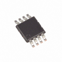
MAX4208AUA+ Maxim Integrated Products, MAX4208AUA+ Datasheet - Page 14

MAX4208AUA+
Manufacturer Part Number
MAX4208AUA+
Description
IC INSTRUMENT AMP PREC 8-UMAX
Manufacturer
Maxim Integrated Products
Datasheet
1.MAX4209EVKIT.pdf
(17 pages)
Specifications of MAX4208AUA+
Amplifier Type
Instrumentation
Number Of Circuits
1
Output Type
Rail-to-Rail
Slew Rate
0.08 V/µs
Gain Bandwidth Product
750kHz
Current - Input Bias
1pA
Voltage - Input Offset
3µV
Current - Supply
1.4mA
Current - Output / Channel
25mA
Voltage - Supply, Single/dual (±)
2.85 V ~ 5.5 V, ±1.425 V ~ 2.25 V
Operating Temperature
-40°C ~ 125°C
Mounting Type
Surface Mount
Package / Case
8-MSOP, Micro8™, 8-uMAX, 8-uSOP,
Number Of Channels
Single
Common Mode Rejection Ratio (min)
106 dB
Input Offset Voltage
0.02 mV
Input Bias Current (max)
0.000001 uA
Operating Supply Voltage
3 V, 5 V
Supply Current
2.3 mA
Maximum Power Dissipation
362 mW
Maximum Operating Temperature
+ 125 C
Minimum Operating Temperature
- 40 C
Mounting Style
SMD/SMT
Maximum Dual Supply Voltage
+/- 2.75 V
Minimum Dual Supply Voltage
+/- 1.425 V
Supply Voltage (max)
5.5 V
Supply Voltage (min)
2.85 V
No. Of Amplifiers
1
Bandwidth
750kHz
Amplifier Output
Rail To Rail
Cmrr
135dB
Supply Voltage Range
± 1.425V To ± 2.75V
Rohs Compliant
Yes
Lead Free Status / RoHS Status
Lead free / RoHS Compliant
-3db Bandwidth
-
Lead Free Status / Rohs Status
Lead free / RoHS Compliant
Ultra-Low Offset/Drift, Precision
Instrumentation Amplifiers with REF Buffer
Good layout technique optimizes performance by
decreasing the amount of stray capacitance at the
instrumentation amplifier’s gain-setting pins (OUT, FB,
and REF). Excess capacitance produces peaking in
the amplifier’s frequency response. To decrease stray
capacitance, minimize trace lengths by placing exter-
nal components as close as possible to the instrumen-
tation amplifier. Unshielded long traces at the inputs of
the instrumentation amplifier degrade the CMRR and
pick-up noise. This produces inaccurate output in high-
gain configurations. Use shielded or coax cables to
connect the inputs of the instrumentation amplifier.
Since the MAX4208/MAX4209 feature ultra-low input
offset voltage, board leakage and thermocouple effects
can easily introduce errors in the input offset voltage
readings when used with high-impedance signal
sources. Minimize board leakage current and thermo-
couple effects by thoroughly cleaning the board and
placing the matching components very close to each
other and with appropriate orientation. For best perfor-
mance, bypass each power supply to ground with a
separate 0.1µF capacitor.
For noisy digital environments, the use of multilayer
PCB with separate ground and power-supply planes is
recommended. Keep digital signals far away from the
sensitive analog inputs.
Refer to the MAX4208 or MAX4209 Evaluation Kit data
sheets for good layout examples.
Figure 3. Limited Common Mode vs. Output Voltage of a
Three Op-Amp INA
14
V
CM-MAX
3/4 V
1/2 V
1/4 V
______________________________________________________________________________________
V
CC
CC
CC
CC
0
V
CM
Power-Supply Bypass and Layout
CLASSIC THREE OP-AMP INA
V
REF
V
= 1/2 V
CC
/2
CC
V
( = GAIN x V
OUT
V
CC
DIFF
+ V
REF
)
The use of indirect current-feedback architecture
makes the MAX4208/MAX4209 ideal for low-side cur-
rent-sensing applications, i.e., where the current in the
circuit ground needs to be measured by means of a
small sense resistor. In these situations, the input com-
mon-mode voltage is allowed to be at or even slightly
below ground (V
If the currents to be measured are bidirectional, con-
nect REFIN/MODE to V
for each direction. If the currents to be measured are
unidirectional, both REFIN/MODE and REF can be tied
to GND. However, VOL limitations can limit low-current
measurement. If currents need to be measured down to
0A, bias REFIN/MODE to a voltage above 0.2V to acti-
vate the internal buffer and to stay above amplifier VOL,
and measure both OUT and REF with a differential
input ADC.
Power management is a critical area in high-perfor-
mance portable devices such as notebook computers.
Modern digital processors and ASICs are using smaller
transistor geometries to increase speed, reduce size,
and also lower their operating core voltages (typically
0.9V to 1.25V). The MAX4208/MAX4209 instrumentation
amplifiers can be used as a nearly zero voltage-drop,
current-sense amplifier (see Figure 5).
Figure 4. Input Common Mode vs. Output Voltage of
MAX4208/MAX4209 Includes 0V (GND)
V
CM-MAX
V
DD
V
CM
0
Low-Side Current-Sense Amplifier
SS
MAX4208/MAX4209
- 0.1V).
V
REF
V
= 1/2 V
DD
DD
/2
Current-Sense Amplifier
Low-Voltage, High-Side
/2 to get full dynamic range
DD
V
DD
V
( = GAIN x V
OUT
DIFF
+ V
REF
)


