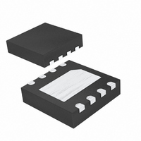
MAX4038ETA+T Maxim Integrated Products, MAX4038ETA+T Datasheet - Page 12

MAX4038ETA+T
Manufacturer Part Number
MAX4038ETA+T
Description
IC OP AMP R-R W/REF 8-TDFN
Manufacturer
Maxim Integrated Products
Datasheet
1.MAX4038ETAT.pdf
(22 pages)
Specifications of MAX4038ETA+T
Amplifier Type
General Purpose
Number Of Circuits
1
Output Type
Rail-to-Rail
Slew Rate
0.004 V/µs
Gain Bandwidth Product
4kHz
Current - Input Bias
1pA
Voltage - Input Offset
200µV
Current - Supply
1.9µA
Current - Output / Channel
13mA
Voltage - Supply, Single/dual (±)
1.4 V ~ 3.6 V
Operating Temperature
-40°C ~ 85°C
Mounting Type
Surface Mount
Package / Case
8-TDFN Exposed Pad
Number Of Channels
2
Voltage Gain Db
108 dB
Common Mode Rejection Ratio (min)
50 dB
Input Offset Voltage
2 mV
Operating Supply Voltage
3 V
Supply Current
0.0025 mA
Maximum Power Dissipation
1951 mW
Maximum Operating Temperature
+ 85 C
Mounting Style
SMD/SMT
Minimum Operating Temperature
- 40 C
Lead Free Status / RoHS Status
Lead free / RoHS Compliant
-3db Bandwidth
-
Lead Free Status / Rohs Status
Details
Other names
MAX4038ETA+T
MAX4038ETA+TTR
MAX4038ETA+TTR
Low I
with +1.2V Buffered Reference
3)
4)
5)
6)
In this application, the MAX4036–MAX4039 supply cur-
rent will vary, depending on the output state of the
comparator.
The MAX4036–MAX4039 operate from a single 1.4V
(MAX4036/MAX4038) or 1.8V (MAX4037/MAX4039) to
3.6V power supply. Bypass V
to ground to minimize noise.
Good layout techniques optimize performance by
decreasing the amount of stray capacitance to the op
amp’s inputs and outputs. To decrease stray capaci-
tance, minimize trace lengths by placing external com-
ponents close to the device.
The exposed paddle (EP) on the TDFN packages of the
MAX4038 and MAX4039 is internally connected to the
device substrate, V
V
exposed paddle is not recommended.
12
SS
R
or leave EP unconnected. Running traces below the
______________________________________________________________________________________
Calculate R1:
Choose the threshold voltage for V
In this example, choose V
Calculate R2:
2
Verify the threshold voltages with these formulas:
V
V
V
IN
IN
THR
=
=
=
rising:
falling:
325
⎡
⎢
⎣
⎡
⎢
⎢
⎣
⎛
⎜
⎝
V
⎛
⎜
⎝
1 2
=
THF
BIAS
V
.
k
REF
Ω
V
V
V
REF
THR
2 0
=
×
R
.
×
SS
1
Power Supplies and Layout
V
210
V
×
. Connect the exposed paddle to
R
THR
=
=
=
1
, +1.4V/800nA, Rail-to-Rail Op Amps
R
⎞
⎟ −
⎠
k
1
1
R
10
Ω
210
3
×
⎞
⎟ −
⎠
−
M
k
×
DD
R
Ω
THR
1
⎛
⎜
⎝
⎛
⎜
⎝
1
Ω
1
R
R
1
V
V
×
1
1
210
with a 0.1µF capacitor
−
HB
DD
= 2.0V.
×
+
R
1
2 4
0 5
R
k
3
.
.
1
Ω
V
3
R
1
DD
V
V
⎤
⎥
⎥
⎦
2
IN
−
+
⎞
⎟
⎠
rising (V
10
R
1
M
1
3
Ω
⎞
⎟
⎠
⎤
⎥
⎦
THR
).
MAX4036 TRANSISTOR COUNT: 49
MAX4037 TRANSISTOR COUNT: 119
MAX4038 TRANSISTOR COUNT: 146
MAX4039 TRANSISTOR COUNT: 146
PROCESS: BiCMOS
Figure 4. Battery Monitoring
- Denotes a package containing lead.
* EP = Exposed pad.
MAX4039EBL-T
MAX4039ETB-T
MAX4039EUB
MAX4036
MAX4037
MAX4038
MAX4039
V
Ordering Information (continued)
BATT
PART
PART
R1
R2
NO. OF AMPLIFIERS
-40°C to +85°C
-40°C to +85°C
-40°C to +85°C
TEMP RANGE
IN+
IN-
REF
V
REF
1
1
2
2
R3
V
SS
Chip Information
V
DD
Selector Guide
V
V
MAX4037
DD
SS
PIN-
PACKAGE
9 UCSP
10 TDFN-EP*
10 µMAX
OUT
REFERENCE
—
—
√
√
V
BGOOD
MARK
TOP
AAN
AEH
—


