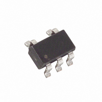
MAX4162EUK+T Maxim Integrated Products, MAX4162EUK+T Datasheet - Page 4

MAX4162EUK+T
Manufacturer Part Number
MAX4162EUK+T
Description
IC OPAMP MICROPWR R-TO-R SOT23-5
Manufacturer
Maxim Integrated Products
Datasheet
1.MAX4162EUKT.pdf
(13 pages)
Specifications of MAX4162EUK+T
Amplifier Type
General Purpose
Number Of Circuits
1
Output Type
Rail-to-Rail
Slew Rate
0.115 V/µs
Gain Bandwidth Product
200kHz
Current - Input Bias
1pA
Voltage - Input Offset
500µV
Current - Supply
25µA
Current - Output / Channel
15mA
Voltage - Supply, Single/dual (±)
2.7 V ~ 10 V, ±1.35 V ~ 5 V
Operating Temperature
-40°C ~ 85°C
Mounting Type
Surface Mount
Package / Case
SOT-23-5, SC-74A, SOT-25
Number Of Channels
1
Common Mode Rejection Ratio (min)
70 dB
Input Offset Voltage
3 mV
Input Bias Current (max)
0.1 nA
Operating Supply Voltage
3 V, 5, V, 9 V
Supply Current
0.025 mA
Maximum Power Dissipation
312 mW
Maximum Operating Temperature
+ 85 C
Minimum Operating Temperature
- 40 C
Dual Supply Voltage
+/- 3 V
Maximum Dual Supply Voltage
+/- 5 V
Minimum Dual Supply Voltage
+/- 1.25 V
Mounting Style
SMD/SMT
Shutdown
No
Supply Voltage (max)
10 V
Supply Voltage (min)
2.5 V
Voltage Gain Db
120 dB
Lead Free Status / RoHS Status
Lead free / RoHS Compliant
-3db Bandwidth
-
Lead Free Status / Rohs Status
Lead free / RoHS Compliant
ELECTRICAL CHARACTERISTICS: 5V Operation (continued)
(V
values are at T
UCSP, Micropower, Single-Supply, 10V,
Rail-to-Rail I/O Op Amps
Note 1: All device specifications are 100% tested at T
Note 2: Input bias current guaranteed by design, not production tested.
4
(V
__________________________________________Typical Operating Characteristics
Total Harmonic Distortion
Slew Rate
Settling Time to 0.1%
Turn-On Time
Input Voltage-Noise Density
Differential Input Capacitance
Input Common-Mode
Capacitance
Internal Charge-Pump
Frequency
Charge-Pump Output
Feedthrough
DD
DD
_______________________________________________________________________________________
30
25
20
15
10
5
0
= 5V, V
= 5V, V
1
design, not production tested.
PARAMETER
2
SS
SS
A
3
vs. SUPPLY VOLTAGE
= 0V, V
= 0V, V
= +25°C.) (Note 1)
SUPPLY CURRENT
SUPPLY VOLTAGE (V)
4
5
CM
CM
6
= V
= V
7
DD
DD
8
/2, T
/2, V
SYMBOL
THD
9
t
A
SR
ON
e
OUT
n
= +25°C, unless otherwise noted.)
10
= V
f = 1kHz, V
V
V
f = 1kHz
DD
OUT
DD
28
26
24
22
20
18
16
14
12
10
/2, R
= 0 to 3V step, V
= 1V to 2V step
-40
A
L
= +25°C. Limits over the extended temperature range are guaranteed by
connected to V
OUT
-20
V
= 2V
CC
vs. TEMPERATURE
CONDITIONS
SUPPLY CURRENT
0
= 3V
TEMPERATURE (°C)
P-P
IN
20
, R
= V
L
40
DD
= 100kΩ, A
DD
V
CC
/2, T
/2, A
60
= 5V
A
V
80
= -40°C to +85°C, unless otherwise noted. Typical
= 1V/V
V
100
= 1V/V
-110
-130
-150
-10
-30
-50
-70
-90
10
50
30
MIN
1
INPUT OFFSET VOLTAGE VARIATION
2
3
vs. SUPPLY VOLTAGE
TYP
0.02
115
700
100
0.7
1.5
70
40
80
SUPPLY VOLTAGE (V)
4
5
MAX
6
7
8
nV/ √ Hz
UNITS
µV
V/ms
kHz
pF
pF
µs
µs
%
9
P-P
10


