MC33179PG ON Semiconductor, MC33179PG Datasheet - Page 5
MC33179PG
Manufacturer Part Number
MC33179PG
Description
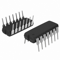
IC OPAMP QUAD LP LO NOISE 14DIP
Manufacturer
ON Semiconductor
Datasheet
1.MC33178PG.pdf
(19 pages)
Specifications of MC33179PG
Amplifier Type
General Purpose
Number Of Circuits
4
Slew Rate
2 V/µs
Gain Bandwidth Product
5MHz
Current - Input Bias
100nA
Voltage - Input Offset
1500µV
Current - Supply
1.7mA
Current - Output / Channel
100mA
Voltage - Supply, Single/dual (±)
4 V ~ 36 V, ±2 V ~ 18 V
Operating Temperature
-40°C ~ 85°C
Mounting Type
Through Hole
Package / Case
14-DIP (0.300", 7.62mm)
Number Of Channels
4
Common Mode Rejection Ratio (min)
80 dB
Input Voltage Range (max)
Positive Rail - 2 V
Input Voltage Range (min)
Negative Rail + 2 V
Input Offset Voltage
3 mV
Input Bias Current (max)
500 nA
Operating Supply Voltage
36 V
Supply Current
1.7 mA
Maximum Operating Temperature
+ 85 C
Minimum Operating Temperature
- 40 C
Dual Supply Voltage
+/- 3 V, +/- 5 V, +/- 9 V
Maximum Dual Supply Voltage
+/- 18 V
Minimum Dual Supply Voltage
+/- 2 V
Mounting Style
Through Hole
Shutdown
No
Technology
Bipolar
Voltage Gain Db
106.02 dB
Lead Free Status / RoHS Status
Lead free / RoHS Compliant
Output Type
-
-3db Bandwidth
-
Lead Free Status / Rohs Status
Lead free / RoHS Compliant
Other names
MC33179PGOS
Available stocks
Company
Part Number
Manufacturer
Quantity
Price
Company:

Part Number:
MC33179PG
Manufacturer:
ON Semiconductor
Quantity:
3 150


AC ELECTRICAL CHARACTERISTICS
Slew Rate
Gain Bandwidth Product (f = 100 kHz)
AC Voltage Gain (R
Unity Gain Bandwidth (Open−Loop) (R
Gain Margin (R
Phase Margin (R
Channel Separation (f = 100 Hz to 20 kHz)
Power Bandwidth (V
Total Harmonic Distortion (R
Open Loop Output Impedance
Differential Input Resistance (V
Differential Input Capacitance (V
Equivalent Input Noise Voltage (R
Equivalent Input Noise Current
2400
2000
1600
1200
(V
(f = 1.0 kHz)
(f = 10 kHz)
(f = 20 kHz)
(V
f = 10 Hz
f = 1.0 kHz
f = 10 Hz
f = 1.0 kHz
800
400
in
O
0
−60 −40 −20
= −10 V to +10 V, R
= 0 V, f = 3.0 MHz, A
MC33178D
MC33178P/9P
MC33179D
Figure 2. Maximum Power Dissipation
L
= 600 W, C
L
= 600 W, C
L
O
T
= 600 W, V
0
A
= 20 V
, AMBIENT TEMPERATURE (°C)
versus Temperature
Characteristics
20
L
V
= 2.0 kW, C
L
L
pp,
= 10 V)
= 0 pF)
L
= 600 W,, V
40
= 0 pF)
CM
O
R
CM
S
L
= 0 V, f = 20 kHz)
= 0 V)
60
= 600 W, THD ≤ 1.0%)
= 100 W,)
= 0 V)
L
L
80 100 120
= 600 W, C
= 100 pF, A
O
= 2.0 V
(V
CC
= +15 V, V
pp
L
V
= 0 pF)
, A
140
= +1.0 V)
V
http://onsemi.com
= +1.0 V)
160
EE
180
= −15 V, T
5
21, 23, 24
22, 23, 24
−1.0
−2.0
−3.0
−4.0
Figure
17, 32
19, 20
4.0
3.0
2.0
1.0
A
18
25
26
27
28
29
0
−55
= 25°C, unless otherwise noted.)
Figure 3. Input Offset Voltage versus
−25
Symbol
Temperature for 3 Typical Units
GBW
BW
THD
A
|Z
BW
SR
A
f
CS
R
C
e
i
VO
n
m
m
O
in
in
n
T
p
|
A
, AMBIENT TEMPERATURE (°C)
0
Unit 1
Unit 2
Unit 3
Min
1.2
2.5
−
−
−
−
−
−
−
−
−
−
−
−
−
−
−
−
25
0.0024
0.014
0.024
−120
0.33
0.15
Typ
150
200
2.0
5.0
3.0
8.0
7.5
50
50
15
60
32
10
75
Max
V
V
R
V
−
−
−
−
−
−
−
−
−
−
−
−
−
−
−
−
−
−
CC
EE
CM
S
= 10 W
= +15 V
= −15 V
= 0 V
100
pA/ Hz
nV/ Hz
V/ms
MHz
MHz
Unit
Deg
kHz
dB
dB
dB
kW
pF
%
W
√
√
125
Related parts for MC33179PG
Image
Part Number
Description
Manufacturer
Datasheet
Request
R

Part Number:
Description:
ON Semiconductor [VOLTAGE REGULATOR]
Manufacturer:
ON Semiconductor
Datasheet:
Part Number:
Description:
357-036-542-201 CARDEDGE 36POS DL .156 BLK LOPRO
Manufacturer:
ON Semiconductor
Datasheet:
Part Number:
Description:
357-036-542-201 CARDEDGE 36POS DL .156 BLK LOPRO
Manufacturer:
ON Semiconductor
Datasheet:
Part Number:
Description:
357-036-542-201 CARDEDGE 36POS DL .156 BLK LOPRO
Manufacturer:
ON Semiconductor
Datasheet:
Part Number:
Description:
357-036-542-201 CARDEDGE 36POS DL .156 BLK LOPRO
Manufacturer:
ON Semiconductor
Datasheet:
Part Number:
Description:
357-036-542-201 CARDEDGE 36POS DL .156 BLK LOPRO
Manufacturer:
ON Semiconductor
Datasheet:
Part Number:
Description:
357-036-542-201 CARDEDGE 36POS DL .156 BLK LOPRO
Manufacturer:
ON Semiconductor
Datasheet:
Part Number:
Description:
357-036-542-201 CARDEDGE 36POS DL .156 BLK LOPRO
Manufacturer:
ON Semiconductor
Datasheet:
Part Number:
Description:
357-036-542-201 CARDEDGE 36POS DL .156 BLK LOPRO
Manufacturer:
ON Semiconductor
Datasheet:
Part Number:
Description:
357-036-542-201 CARDEDGE 36POS DL .156 BLK LOPRO
Manufacturer:
ON Semiconductor
Datasheet:
Part Number:
Description:
357-036-542-201 CARDEDGE 36POS DL .156 BLK LOPRO
Manufacturer:
ON Semiconductor
Datasheet:
Part Number:
Description:
Manufacturer:
ON Semiconductor
Datasheet:
Part Number:
Description:
Manufacturer:
ON Semiconductor
Datasheet:
Part Number:
Description:
Manufacturer:
ON Semiconductor
Datasheet: