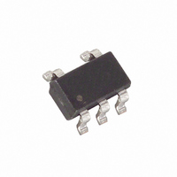
MAX4321EUK+T Maxim Integrated Products, MAX4321EUK+T Datasheet - Page 7

MAX4321EUK+T
Manufacturer Part Number
MAX4321EUK+T
Description
IC OP AMP R-R I/O LV SOT23-5
Manufacturer
Maxim Integrated Products
Datasheet
1.MAX4321EUKT.pdf
(12 pages)
Specifications of MAX4321EUK+T
Amplifier Type
General Purpose
Number Of Circuits
1
Output Type
Rail-to-Rail
Slew Rate
2 V/µs
Gain Bandwidth Product
5MHz
Current - Input Bias
50nA
Voltage - Input Offset
1200µV
Current - Supply
725µA
Current - Output / Channel
50mA
Voltage - Supply, Single/dual (±)
2.4 V ~ 6.5 V, ±1.2 V ~ 3.25 V
Operating Temperature
-40°C ~ 85°C
Mounting Type
Surface Mount
Package / Case
SOT-23-5, SC-74A, SOT-25
Number Of Channels
1
Voltage Gain Db
103 dB
Common Mode Rejection Ratio (min)
60 dB
Input Offset Voltage
3.5 mV
Operating Supply Voltage
3 V, 5 V
Supply Current
0.725 mA
Maximum Power Dissipation
571 mW
Maximum Operating Temperature
+ 85 C
Mounting Style
SMD/SMT
Maximum Dual Supply Voltage
+/- 3.25 V
Minimum Operating Temperature
- 40 C
Lead Free Status / RoHS Status
Lead free / RoHS Compliant
-3db Bandwidth
-
Lead Free Status / Rohs Status
Details
Other names
MAX4321EUK+T
MAX4321EUK+TTR
MAX4321EUK+TTR
__________ Applications Information
The MAX4321 high-speed amplifier has rail-to-rail input
and output stages designed for low-voltage, single-
supply operation. The input stage consists of separate
NPN and PNP differential stages, which combine to
provide an input common-mode range extending to the
supply rails. The PNP stage is active for input voltages
close to the negative rail, and the NPN stage is active
for input voltages near the positive rail. The switchover
transition region, which occurs near V
extended to minimize the slight degradation in CMRR
caused by the mismatch of the input pairs. Its low offset
voltage, high bandwidth, and rail-to-rail common-mode
range makes this op amp an excellent choice for preci-
sion, low-voltage, data-acquisition systems.
Since the input stage switches between the NPN and
PNP pairs, the input bias current changes polarity as
the input voltage passes through the transition region.
To reduce the offset error caused by input bias cur-
Figure 1a. Reducing Offset Error Due to Bias Current
(Noninverting)
Figure 2. Input Protection Circuit
R3 = R1
R2
MAX4321
_______________________________________________________________________________________
R3
R1
Rail-to-Rail Input Stage
Low-Cost, Low-Voltage, Rail-to-Rail,
1k
1k
Input/Output, SOT23 5MHz Op Amp
R2
CC
/ 2, has been
rents flowing through external source impedances,
match the effective impedance seen by each input
(Figures 1a, 1b). High source impedances, together
with the input capacitance, can create a parasitic pole
that produces an underdamped signal response.
Reducing the input impedance or placing a small (2pF
to 10pF) capacitor across the feedback resistor
improves the response.
The MAX4321’s inputs are protected from large differen-
tial input voltages by 1kΩ series resistors and back-to-
back triple diodes across the inputs (Figure 2). For
differential input voltages less than 1.8V, the input resis-
tance is typically 500kΩ. For differential input voltages
greater than 1.8V, the input resistance is approximately
2kΩ, and the input bias current is determined by the fol-
lowing equation:
Figure 1b. Reducing Offset Error Due to Bias Current
(Inverting)
R3 = R1
R2
MAX4321
I
BIAS
R1
R3
=
V
DIFF
2k
- 1.8V
Ω
R2
7


