LMH6502MA/NOPB National Semiconductor, LMH6502MA/NOPB Datasheet - Page 2
LMH6502MA/NOPB
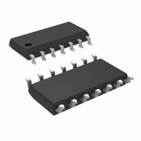
Manufacturer Part Number
LMH6502MA/NOPB
Description
IC AMP VARIABLE GAIN 14-SOIC
Manufacturer
National Semiconductor
Series
LMH®r
Type
Variable Gain Amplifierr
Datasheet
1.LMH6502MANOPB.pdf
(19 pages)
Specifications of LMH6502MA/NOPB
Amplifier Type
Variable Gain
Number Of Circuits
1
Slew Rate
1800 V/µs
-3db Bandwidth
130MHz
Current - Input Bias
9µA
Current - Supply
27mA
Current - Output / Channel
90mA
Voltage - Supply, Single/dual (±)
5 V ~ 12 V, ±2.5 V ~ 6 V
Operating Temperature
-40°C ~ 85°C
Mounting Type
Surface Mount
Package / Case
14-SOIC (3.9mm Width), 14-SOL
Number Of Channels
1
Number Of Elements
1
Power Supply Requirement
Single/Dual
Common Mode Rejection Ratio
72dB
Unity Gain Bandwidth Product (typ)
100MHz
Single Supply Voltage (typ)
9V
Dual Supply Voltage (typ)
±3/±5V
Power Supply Rejection Ratio
69dB
Rail/rail I/o Type
No
Single Supply Voltage (min)
5V
Single Supply Voltage (max)
12V
Dual Supply Voltage (min)
±2.5V
Dual Supply Voltage (max)
±6V
Operating Temp Range
-40C to 85C
Operating Temperature Classification
Industrial
Mounting
Surface Mount
Pin Count
14
Package Type
SOIC N
For Use With
CLC730033 - EVAL BOARD AMP FOR 14-SOIC
Lead Free Status / RoHS Status
Lead free / RoHS Compliant
Output Type
-
Gain Bandwidth Product
-
Voltage - Input Offset
-
Lead Free Status / Rohs Status
Compliant
Other names
*LMH6502MA
*LMH6502MA/NOPB
LMH6502MA
*LMH6502MA/NOPB
LMH6502MA
Available stocks
Company
Part Number
Manufacturer
Quantity
Price

Part Number:
LMH6502MA/NOPB
Manufacturer:
NS/国半
Quantity:
20 000


www.national.com
Frequency Domain Response
BW
GF
Att Range Flat Band (Relative to Max Gain)
BW
Control
PL
G Delay
CT (dB)
GR
Time Domain Response
t
OS %
SR
∆ G Rate
Distortion & Noise Performance
HD2
HD3
THD
En tot
I
DG
DP
r
N
Symbol
, t
Absolute Maximum Ratings
If Military/Aerospace specified devices are required,
please contact the National Semiconductor Sales Office/
Distributors for availability and specifications.
Electrical Characteristics
Unless otherwise specified, all limits guaranteed for T
V
ESD Tolerance (Note 4):
Input Current
V
Output Current
Supply Voltages (V
Voltage at Input/ Output pins
Storage Temperature Range
f
IN_DIFF
IN
Human Body
Machine Model
Differential
=
-3dB Bandwidth
Gain Flatness
Attenuation Range (Note 14)
Gain control Bandwidth
Linear Phase Deviation
Group Delay
Feed-through
Gain Adjustment Range
Rise and Fall Time
Overshoot
Slew Rate
Gain Change Rate
2
3
Total Harmonic Distortion
Total Equivalent Input Noise
Input Noise Current
Differential Gain
Differential Phase
±
nd
rd
0.1V, R
Harmonic Distortion
Harmonic Distortion
+
L
- V
= 100Ω, V
Parameter
−
)
G
= +2V. Boldface limits apply at the temperature extremes.
V
+
−65˚C to +150˚C
(Note 2)
120mA (Note 3)
+0.8V,V
(Note 1)
V
V
V
0.6V ≤ V
V
DC to 60MHz
DC to 130MHz
V
Referred)
f
f
0.5V Step
0.5V Step
4V Step
V
Output
2V
2V
2V
1MHz to 150MHz
1MHz to 150MHz
f = 4.43MHz, R
Neg. Sync
f = 4.43MHz, R
Neg. Sync
±
±
OUT
OUT
OUT
G
G
<
<
IN
±
0.2dB, f
0.1dB, f
PP
PP
PP
(V
−
±
= 1V (Note 13)
= 0V, 30MHz (Output
10MHz
30MHz
= 0.3V, 10%-90% of Final
- 0.8V
, 20MHz
, 20MHz
, 20MHz
10mA
+
12.6V
200V
<
<
<
J
2KV
-V
= 25˚C, V
0.5
0.5
0.5V
G
−
Conditions
<
<
)
≤ 2V,
PP
PP
30MHz
30MHz
PP
, A
2
L
L
V(MAX)
±
= 150Ω,
= 150Ω,
S
0.3dB
Operating Ratings
=
Junction Temperature
Soldering Information:
Supply Voltages (V
Temperature Range
Thermal Resistance:
±
Infrared or Convection (20 sec)
Wave Soldering (10 sec)
14-Pin SOIC
14-Pin TSSOP
5V, A
= 100
V(MAX)
(Note 6)
= 10, V
Min
+
- V
CM
−
)
(Note 6)
= 0V, R
45˚C/W
51˚C/W
1800
0.34
0.10
Typ
−47
−55
−57
−53
130
100
7.5
1.5
2.5
2.2
4.8
7.7
2.4
50
30
16
72
67
10
(θ
(Note 1)
JC
)
F
= 1kΩ, R
(Note 6)
Max
−40˚C to +85˚C
138˚C/W
160˚C/W
G
(θ
5V to 12V
= 174Ω,
JA
+150˚C
)
235˚C
260˚C
nV/
pA/
Units
dB/ns
MHz
MHz
MHz
V/µs
deg
dBc
dBc
dBc
deg
dB
dB
dB
ns
ns
%
%
Related parts for LMH6502MA/NOPB
Image
Part Number
Description
Manufacturer
Datasheet
Request
R

Part Number:
Description:
Operational Amplifier (Op-Amp) IC
Manufacturer:
National Semiconductor

Part Number:
Description:
National Semiconductor [8-Bit D/A Converter]
Manufacturer:
National Semiconductor
Datasheet:
Part Number:
Description:
National Semiconductor [Media Coprocessor]
Manufacturer:
National Semiconductor
Datasheet:
Part Number:
Description:
Digitally Controlled Tone and Volume Circuit with Stereo Audio Power Amplifier, Microphone Preamp Stage and National 3D Sound
Manufacturer:
National Semiconductor
Datasheet:
Part Number:
Description:
Digitally Controlled Tone and Volume Circuit with Stereo Audio Power Amplifier, Microphone Preamp Stage and National 3D Sound
Manufacturer:
National Semiconductor
Datasheet:
Part Number:
Description:
AC97 Rev 2 Codec with Sample Rate Conversion and National 3D Sound
Manufacturer:
National Semiconductor
Part Number:
Description:
Manufacturer:
National Semiconductor
Datasheet:
Part Number:
Description:
Manufacturer:
National Semiconductor
Datasheet:
Part Number:
Description:
General Purpose, Low Voltage, Low Power, Rail-to-Rail Output Operational Amplifiers
Manufacturer:
National Semiconductor
Datasheet:
Part Number:
Description:
8-bit 20 MSPS flash A/D converter.
Manufacturer:
National Semiconductor
Datasheet:
Part Number:
Description:
Low Noise Quad Operational Amplifier
Manufacturer:
National Semiconductor
Datasheet:
Part Number:
Description:
Quad Differential Line Receivers
Manufacturer:
National Semiconductor
Datasheet:
Part Number:
Description:
Quad High Speed Trapezoidal? Bus Transceiver
Manufacturer:
National Semiconductor
Datasheet:
Part Number:
Description:
Dual Line Receiver
Manufacturer:
National Semiconductor
Datasheet: