LMH6503MA/NOPB National Semiconductor, LMH6503MA/NOPB Datasheet - Page 17

LMH6503MA/NOPB
Manufacturer Part Number
LMH6503MA/NOPB
Description
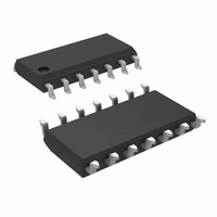
IC AMP VARIABLE GAIN 14-SOIC
Manufacturer
National Semiconductor
Series
LMH®r
Datasheet
1.LMH6503MANOPB.pdf
(20 pages)
Specifications of LMH6503MA/NOPB
Amplifier Type
Variable Gain
Number Of Circuits
1
Slew Rate
1800 V/µs
-3db Bandwidth
135MHz
Current - Input Bias
11µA
Current - Supply
37mA
Current - Output / Channel
90mA
Voltage - Supply, Single/dual (±)
5 V ~ 12 V, ±2.5 V ~ 6 V
Operating Temperature
-40°C ~ 85°C
Mounting Type
Surface Mount
Package / Case
14-SOIC (3.9mm Width), 14-SOL
For Use With
CLC730033 - EVAL BOARD AMP FOR 14-SOIC
Lead Free Status / RoHS Status
Lead free / RoHS Compliant
Output Type
-
Gain Bandwidth Product
-
Voltage - Input Offset
-
Other names
*LMH6503MA
LMH6503MA
LMH6503MA
Application Information
OPERATING AT LOWER SUPPLY VOLTAGES
The LMH6503 is rated for operation down to 5V supplies (V
- V
CMRR, PSRR, Gain vs. V
tion, at lower supplies:
a) V
b) V
±
2.5V within the data sheet (i.e. Frequency Response,
FIGURE 8. Transformer Coupled Single Supply VGA
−
V
0.5V (V
same time, gain cut-off (V
- 1V with V
Table 1 shows the approximate expressions for various
V
duced. This is due to limitations within the device arising
from transistor headroom. Beyond this limit, device per-
formance will be affected (non-destructive). Referring to
Figure 9, note that with V
is approaching V
duced by 1dB. This means that operating under these
conditions has reduced the maximum permissible voltage
on V
supply voltages are asymmetrical, reference Figure 9 and
). There are some specifications shown for operation at
V
G
G_MAX
G
V
V
G_LIMIT
G_MAX
G_MIN
G_MID
voltages as a function of V
V
range constricts. Referring to Figure 9, note that
G
G
to a level below what is needed to get Max gain. If
S
Table 1: V
(V
=
(maximum permissible voltage on V
G
±
S
2.5V) compared to 1.0V for V
=
voltage required to get maximum gain) is
±
5V.
Gain Cut-off
G_MAX
Definition
G
A
A
Definition Based on V
VMAX
VMAX
G
, etc.). Compared to
+
G_MIN
and already "Max gain" is re-
/2
= 2.5V, and V
-
) would shift to −0.5V from
:
Expression (V)
(Continued)
−
−0.2 x V
0.2 x V
= −4V, V
S
=
−
0
±
±
5V opera-
5V. At the
G
−
−
) is re-
20073936
G_LIMIT
+
17
c) "Max_gain" reduces. There is an intrinsic reduction in
Similar plots for V
comparison and reference.
Figure 10 plots to make sure the region of operation is not
overly restricted by the "pinching" of V
_MAX
max gain when the total supply voltage is reduced (see
Typical Performance Characteristics plots for Gain vs. V
(V
mechanism described in "b" above and shown in Figure
9.
FIGURE 10. V
FIGURE 9. V
S
=
curves.
±
2.5V). In addition, there is the more drastic
+
G_MAX
= 5V operation are shown in Figure 10 for
G_MAX
(V
, V
(V
, V
+
+
G_LIMIT
= 2.5V)
G_LIMIT
= 5V)
, & Max-gain vs. V
, & Max-gain vs. V
G_LIMIT
www.national.com
, and V
20073926
20073925
-
-
G -
G


