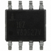
HFA1130IBZ Intersil, HFA1130IBZ Datasheet - Page 4

HFA1130IBZ
Manufacturer Part Number
HFA1130IBZ
Description
IC OP AMP 850MHZ CFB 8-SOIC
Manufacturer
Intersil
Datasheet
1.HFA1130IBZ.pdf
(12 pages)
Specifications of HFA1130IBZ
Amplifier Type
Current Feedback
Number Of Circuits
1
Slew Rate
2300 V/µs
-3db Bandwidth
850MHz
Current - Input Bias
25µA
Voltage - Input Offset
2000µV
Current - Supply
21mA
Current - Output / Channel
60mA
Voltage - Supply, Single/dual (±)
±4.5 V ~ 5.5 V
Operating Temperature
-40°C ~ 85°C
Mounting Type
Surface Mount
Package / Case
8-SOIC (3.9mm Width)
Lead Free Status / RoHS Status
Lead free / RoHS Compliant
Output Type
-
Gain Bandwidth Product
-
Available stocks
Company
Part Number
Manufacturer
Quantity
Price
Company:
Part Number:
HFA1130IBZ
Manufacturer:
Intersil
Quantity:
86
Electrical Specifications
NOTES:
Application Information
Optimum Feedback Resistor (R
The enclosed plots of inverting and non-inverting frequency
response detail the performance of the HFA1130 in various
gains. Although the bandwidth dependency on A
severe as that of a voltage feedback amplifier, there is an
appreciable decrease in bandwidth at higher gains. This
decrease can be minimized by taking advantage of the current
feedback amplifier’s unique relationship between bandwidth
and R
resistor, even for unity gain applications, and the R
conjunction with the internal compensation capacitor, sets the
dominant pole of the frequency response. Thus, the
amplifier’s bandwidth is inversely proportional to R
HFA1130 design is optimized for a 510Ω R
Decreasing R
resulting in excessive peaking and overshoot (Note:
Capacitive feedback causes the same problems due to the
feedback impedance decrease at higher frequencies). At
higher gains the amplifier is more stable, so R
decreased in a trade-off of stability for bandwidth. The table
below lists recommended R
expected bandwidth.
Clamp Operation
General
The HFA1130 features user programmable output clamps to
limit output voltage excursions. Clamping action is obtained
by applying voltages to the V
5) of the amplifier. V
sets the lower clamp level. If the amplifier tries to drive the
output above V
Negative Clamp Range
Positive Clamp Range
Clamp Input Bias Current
Clamp Input Bandwidth
2. Test Level: A. Production Tested; B. Typical or Guaranteed Limit Based on Characterization; C. Design Typical for Information Only.
3. See Typical Performance Curves for more information.
F
. All current feedback amplifiers require a feedback
PARAMETER
F
A
+10
+19
in a unity gain application decreases stability,
H
+1
+2
+5
-1
CL
, or below V
H
sets the upper output limit, while V
R
F
510
430
360
150
180
270
F
values for various gains, and the
L
(Ω)
H
, the clamp circuitry limits the
4
and V
V
SUPPLY
L
F
BW (MHz)
terminals (pins 8 and
V
)
H
850
580
670
520
240
125
= ±5V, A
F
or V
CONDITIONS
, at a gain of +1.
F
L
TEST
can be
= 100mV
CL
V
F
F
= +1, R
. The
isn’t as
, in
P-P
F
L
= 510Ω, R
HFA1130
(NOTE 2)
LEVEL
TEST
B
B
A
B
L
= 100Ω, Unless Otherwise Specified (Continued)
output voltage at V
respectively. The low input bias currents of the clamp pins
allow them to be driven by simple resistive divider circuits, or
active elements such as amplifiers or DACs.
Clamp Circuitry
Figure 1 shows a simplified schematic of the HFA1130 input
stage, and the high clamp (V
feedback amplifiers, there is a unity gain buffer (Q
between the positive and negative inputs. This buffer forces -IN
to track +IN, and sets up a slewing current of (V
This current is mirrored onto the high impedance node (Z) by
Q
via another unity gain buffer. If no clamping is utilized, the high
impedance node may swing within the limits defined by Q
Q
current flowing through -IN is reduced to only that small current
(-I
Tracing the path from V
clamp voltage on the high impedance node. V
by 2V
Q
+IN
X3
N4
P5
TEMP.
BIAS
(°C)
FIGURE 1. HFA1130 SIMPLIFIED V
25
25
25
25
-Q
. Note that when the output reaches it’s quiescent value, the
begins to conduct whenever the high impedance node
BE
) required to keep the output at the final voltage.
X4
, where it is converted to a voltage and fed to the output
(Q
Q
Q
N6
V-
V+
N1
P1
MIN
Q
Q
and Q
-
-
-
-
P3
N3
V-
H
Q
I
Q
CLAMP
N2
P2
or V
P6
V+
-IN
-5.0 to +2.0
-2.0 to +5.0
) to set up the base voltage on Q
H
L
to Z illustrates the effect of the
TYP
500
(± the clamp accuracy),
H
50
) circuitry. As with all current
Q
Q
N4
P4
Z
Q
Q
N5
P5
(EXTERNAL)
H
CLAMP CIRCUITRY
MAX
+1
200
R
-
-
-
F
Q
Q
N6
P6
-IN
FOR V
H
X1
- V
decreases
200Ω
(30K
50K
- Q
OUT
L
UNITS
July 15, 2005
)
MHz
X2
µA
V
V
P4
FN3369.4
)/R
V
)
R
H
V
P5
and
1
OUT
F
.
.


