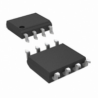
LMH6504MA/NOPB National Semiconductor, LMH6504MA/NOPB Datasheet

LMH6504MA/NOPB
Specifications of LMH6504MA/NOPB
*LMH6504MA/NOPB
LMH6504MA
Related parts for LMH6504MA/NOPB
LMH6504MA/NOPB Summary of contents
Page 1
... AGC applications. For linear gain control applications, see LMH6503 data sheet. The combination of minimal external components and small outline packages (SO8 and MSOP8) allows the LMH6504 to be used in space-constrained applications. Gain vs LMH is a trademark of National Semiconductor Corporation. ™ © 2006 National Semiconductor Corporation Features ± 5V 25˚ ...
Page 2
... Absolute Maximum Ratings If Military/Aerospace specified devices are required, please contact the National Semiconductor Sales Office/ Distributors for availability and specifications. ESD Tolerance (Note 4): Human Body Model Machine Model Input Current Output Current + − Supply Voltages ( Voltage at Input/ Output pins Storage Temperature Range ...
Page 3
Electrical Characteristics Unless otherwise specified, all limits guaranteed for T ± 0.1V 100Ω +2V. Boldface limits apply at the temperature extremes Symbol Parameter DC & Miscellaneous Performance GACCU Gain Accuracy (See Application Note) G ...
Page 4
Electrical Characteristics Note 1: Absolute Maximum Ratings indicate limits beyond which damage to the device may occur. Operating Ratings indicate conditions for which the device is intended to be functional, but specific performance is not guaranteed. For guaranteed specifications, see ...
Page 5
Typical Performance Characteristics kΩ 100Ω GMAX F G Frequency Response Over Temperature Frequency Response (A Frequency Response for Various V (Large Signal) Unless otherwise specified 0.1V, input ...
Page 6
Typical Performance Characteristics kΩ 100Ω GMAX F G Gain Control Frequency Response I vs PSRR www.national.com Unless otherwise specified 0.1V, input terminated in 50Ω. ...
Page 7
Typical Performance Characteristics kΩ 100Ω GMAX Feed through Isolation for Various Gain vs. V Including Limits G Unless otherwise specified: ...
Page 8
Typical Performance Characteristics kΩ 100Ω GMAX F G Output Offset Voltage vs Distribution of Output Offset Voltage Output Noise Density vs. Frequency www.national.com Unless otherwise specified: V ...
Page 9
Typical Performance Characteristics kΩ 100Ω GMAX Input Referred Noise Density vs. Frequency Output Voltage vs. Output Current (Sourcing) HD vs. P OUT Unless otherwise specified: V ...
Page 10
Typical Performance Characteristics kΩ 100Ω GMAX F G THD vs. P OUT THD vs. Gain V Bias Current vs www.national.com Unless otherwise specified 0.1V, input ...
Page 11
Typical Performance Characteristics kΩ 100Ω GMAX Step Response Plot Gain vs. V Step G Unless otherwise specified 0.1V, input terminated in 50Ω ...
Page 12
Application Information GENERAL DESCRIPTION The key features of the LMH6504 are: • Low power • Broad voltage controlled gain and attenuation range (From A down to complete cutoff) VMAX • Bandwidth independent, resistor programmable gain range ( • ...
Page 13
Application Information GAIN ACCURACY Gain accuracy is defined as the actual gain compared against the theoretical gain at a certain V pressed in dB) (See Figure 2). Theoretical gain is given by: Eq. 3 Where K = 0.965 (nominal) N ...
Page 14
Application Information LMH6504 GAIN CONTROL FUNCTION In the plot, Gain vs can see the gain as a function of G the control voltage. The “Gain (V/V)” plot, sometimes re- ferred to as the S-curve, is the linear ...
Page 15
... Digitally variable gain control can be easily realized by driv- ing the LMH6504’s gain control input with a digital-to-analog converter (DAC). Figure 7 illustrates such an application. This circuit employs National Semiconductor’s eight-bit DAC0830, the LMC8101 MOS input op-amp (Rail-to-Rail Input/Output), and the LMH6504 VGA. With V the circuit provides gain control in 256 steps with ...
Page 16
Application Information Signal frequencies must not reach the gain control port of the LMH6504, or the output signal will be distorted (modulated by itself). A fast settling AGC needs additional filtering be- yond the integrator stage to block signal frequencies. ...
Page 17
... National Semiconductor suggests the following evaluation . Para- board as a guide for high frequency layout and as an aid in G device testing and characterization: Device LMH6504 The evaluation board is shipped when a device sample request is placed with National Semiconductor. 17 20084360 can also be isolated from L Package Evaluation Board Part Number ...
Page 18
Physical Dimensions www.national.com inches (millimeters) unless otherwise noted 8-Pin SOIC NS Package Number M08A 8-Pin MSOP NS Package Number MUA08A 18 ...
Page 19
... BANNED SUBSTANCE COMPLIANCE National Semiconductor follows the provisions of the Product Stewardship Guide for Customers (CSP-9-111C2) and Banned Substances and Materials of Interest Specification (CSP-9-111S2) for regulatory environmental compliance. Details may be found at: www.national.com/quality/green. ...


