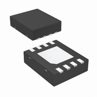
LMH6552SD/NOPB National Semiconductor, LMH6552SD/NOPB Datasheet - Page 16

LMH6552SD/NOPB
Manufacturer Part Number
LMH6552SD/NOPB
Description
IC AMP DIFF 1.5GHZ 1CN 8-LLP
Manufacturer
National Semiconductor
Series
LMH®, PowerWise®r
Datasheet
1.LMH6552SDEVAL.pdf
(22 pages)
Specifications of LMH6552SD/NOPB
Amplifier Type
Differential
Number Of Circuits
1
Output Type
Differential
Slew Rate
3800 V/µs
-3db Bandwidth
1.5GHz
Current - Input Bias
60µA
Voltage - Input Offset
1500µV
Current - Supply
22.5mA
Current - Output / Channel
80mA
Voltage - Supply, Single/dual (±)
4.5 V ~ 12 V, ±2.25 V ~ 6 V
Operating Temperature
-40°C ~ 85°C
Mounting Type
Surface Mount
Package / Case
8-LLP
For Use With
LMH6552SDEVAL - BOARD EVALUATION FOR LMH6552
Lead Free Status / RoHS Status
Lead free / RoHS Compliant
Gain Bandwidth Product
-
Other names
LMH6552SD
LMH6552SD
LMH6552SDTR
LMH6552SD
LMH6552SDTR
www.national.com
SPLIT SUPPLY OPERATION
For optimum performance, split supply operation is recom-
mended using +5V and −5V supplies; however, operation is
possible on split supplies as low as +2.25V and −2.25V and
as high as +6V and −6V. Provided the total supply voltage
does not exceed the 4.5V to 12V operating specification, non-
symmetric supply operation is also possible and in some
cases advantageous. For example , if a 5V DC coupled op-
eration is required for low power dissipation but the amplifier
input common mode range prevents this operation, it is still
possible with split supplies of (V
(V
plifier input common mode range to suit the application.
OUTPUT NOISE PERFORMANCE AND MEASUREMENT
Unlike differential amplifiers based on voltage feedback ar-
chitectures, noise sources internal to the LMH6552 refer to
the inputs largely as current sources, hence the low input re-
ferred voltage noise and relatively higher input referred cur-
rent noise. The output noise is therefore more strongly
coupled to the value of the feedback resistor and not to the
closed loop gain, as would be the case with a voltage feed-
back differential amplifier. This allows operation of the
LMH6552 at much higher gain without incurring a substantial
noise performance penalty, simply by choosing a suitable
feedback resistor.
Figure 6
figure for the LMH6552 in a 50Ω system. An R
275Ω is chosen for the SOIC package to minimize output
noise while simultaneously allowing both high gain (9 V/V)
and proper 50Ω input termination. Refer to the section titled
Single Ended Input Operation for calculation of resistor and
gain values. Noise figure values at various frequencies are
shown in the plot titled Noise Figure in the Typical Perfor-
mance Characteristics section.
DRIVING ANALOG TO DIGITAL CONVERTERS
Analog-to-digital converters present challenging load condi-
tions. They typically have high impedance inputs with large
and often variable capacitive components. As well, there are
usually current spikes associated with switched capacitor or
sample and hold circuits.
of the LMH6552 driving the ADC12DL080. The two 125Ω re-
sistors serve to isolate the capacitive loading of the ADC from
the amplifier and ensure stability. In addition, the resistors,
along with a 2.2 pF capacitor across the outputs (in parallel
with the ADC input capacitance), form a low pass anti-aliasing
filter with a pole frequency of about 60 MHz. For switched
+
) - (V
FIGURE 6. Noise Figure Circuit Configuration
−
shows a circuit configuration used to measure noise
) = 5V and V
+
and V
Figure 7
−
are selected to center the am-
shows a combination circuit
+
) and (V
−
F
). Where
value of
30003550
16
capacitor input ADCs, the input capacitance will vary based
on the clock cycle, as the ADC switches between the sample
and hold mode. See your particular ADC's datasheet for de-
tails.
Figure 8
cy for the LMH6552 and ADC12DL080 combination circuit
with the ADC input signal level at −1 dBFS. The ADC12DL080
is a dual 12-bit ADC with maximum sampling rate of 80 MSPS.
The amplifier is configured to provide a gain of 2 V/V in single
to differential mode. An external band-pass filter is inserted in
series between the input signal source and the amplifier to
reduce harmonics and noise from the signal generator. In or-
der to properly match the input impedance seen at the
LMH6552 amplifier inputs, R
proper input balance.
Figure 9
the ADC14DS105. The ADC14DS105 is a dual channel 14-
bit ADC with a sampling rate of 105 MSPS. The circuit in
Figure 9
nH inductor along with the 22 pF capacitor across the differ-
ential outputs of the LMH6552. The filter has a pole frequency
of about 50 MHz.
SNR performance over frequency with a −1 dBFs input signal
and a sampling rate of 1000 MSPS.
FIGURE 8. LMH6552/ADC12DL080 SFDR and SNR
shows the SFDR and SNR performance vs. frequen-
has a 2nd order low-pass LC filter formed by the 620
shows a combination circuit of the LMH6552 driving
FIGURE 7. Driving a 12-bit ADC
Performance vs. Frequency
Figure 10
shows the combined SFDR and
M
is chosen to match Z
30003540
S
|| R
30003505
T
for


