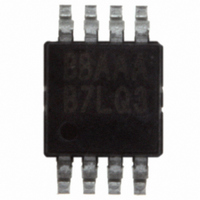
EL5220CYZ Intersil, EL5220CYZ Datasheet - Page 12

EL5220CYZ
Manufacturer Part Number
EL5220CYZ
Description
IC OP AMP 12MHZ R-R 8-MSOP
Manufacturer
Intersil
Datasheet
1.EL5220CYZ.pdf
(20 pages)
Specifications of EL5220CYZ
Amplifier Type
Voltage Feedback
Number Of Circuits
2
Output Type
Rail-to-Rail
Slew Rate
10 V/µs
Gain Bandwidth Product
8MHz
-3db Bandwidth
12MHz
Current - Input Bias
2nA
Voltage - Input Offset
2000µV
Current - Supply
500µA
Current - Output / Channel
30mA
Voltage - Supply, Single/dual (±)
4.5 V ~ 16.5 V, ±2.25 V ~ 8.25 V
Operating Temperature
-40°C ~ 85°C
Mounting Type
Surface Mount
Package / Case
8-MSOP, Micro8™, 8-uMAX, 8-uSOP,
Lead Free Status / RoHS Status
Lead free / RoHS Compliant
Available stocks
Company
Part Number
Manufacturer
Quantity
Price
Company:
Part Number:
EL5220CYZ
Manufacturer:
ROHM
Quantity:
29 562
Part Number:
EL5220CYZ
Manufacturer:
INT
Quantity:
20 000
Company:
Part Number:
EL5220CYZ-T13
Manufacturer:
INTERSIL
Quantity:
38 188
Company:
Part Number:
EL5220CYZ-T13
Manufacturer:
INTERSIL
Quantity:
26 283
Part Number:
EL5220CYZ-T13
Manufacturer:
INTERSIL
Quantity:
20 000
Applications Information
Product Description
The EL5120, EL5220, and EL5420 voltage feedback
amplifiers are fabricated using a high voltage CMOS
process. They exhibit rail-to-rail input and output capability,
they are unity gain stable, and have low power consumption
(500µA per amplifier). These features make the EL5120,
EL5220, and EL5420 ideal for a wide range of general-
purpose applications. Connected in voltage follower mode
and driving a load of 10kΩ and 12pF, the EL5120, EL5220,
and EL5420 have a -3dB bandwidth of 12MHz while
maintaining a 10V/µs slew rate. The EL5120 is a single
amplifier, the EL5220 is a dual amplifier, and the EL5420 is a
quad amplifier.
Operating Voltage, Input, and Output
The EL5120, EL5220, and EL5420 are specified with a
single nominal supply voltage from 5V to 15V or a split
supply with its total range from 5V to 15V. Correct operation
is guaranteed for a supply range of 4.5V to 16.5V. Most
EL5120, EL5220, and EL5420 specifications are stable over
both the full supply range and operating temperatures of
-40°C to +85°C. Parameter variations with operating voltage
and/or temperature are shown in the typical performance
curves.
The input common-mode voltage range of the EL5120,
EL5220, and EL5420 extends 500mV beyond the supply
rails. The output swings of the EL5120, EL5220, and
EL5420 typically extend to within 80mV of positive and
negative supply rails with load currents of 5mA. Decreasing
load currents will extend the output voltage range even
closer to the supply rails. Figure 25 shows the input and
output waveforms for the device in the unity-gain
configuration. Operation is from ±5V supply with a 10kΩ load
connected to GND. The input is a 10V
output voltage is approximately 9.985V
Short Circuit Current Limit
The EL5120, EL5220, and EL5420 will limit the short circuit
current to ±120mA if the output is directly shorted to the
positive or the negative supply. If an output is shorted
FIGURE 25. OPERATION WITH RAIL-TO-RAIL INPUT AND
OUTPUT
V
T
A
V
A
S
V
IN
= +25°C
= ±5V
= 1
= 10V
12
P-P
P-P
P-P
.
sinusoid. The
EL5120, EL5220, EL5420
indefinitely, the power dissipation could easily increase such
that the device may be damaged. Maximum reliability is
maintained if the output continuous current never exceeds
±30mA. This limit is set by the design of the internal metal
interconnects.
Output Phase Reversal
The EL5120, EL5220, and EL5420 are immune to phase
reversal as long as the input voltage is limited from (V
-0.5V to (V
of the device with the input voltage driven beyond the supply
rails. Although the device's output will not change phase, the
input's overvoltage should be avoided. If an input voltage
exceeds supply voltage by more than 0.6V, electrostatic
protection diodes placed in the input stage of the device
begin to conduct and overvoltage damage could occur.
Power Dissipation
With the high-output drive capability of the EL5120, EL5220,
and EL5420 amplifiers, it is possible to exceed the +125°C
“absolute-maximum junction temperature” under certain load
current conditions. Therefore, it is important to calculate the
maximum junction temperature for the application to
determine if load conditions need to be modified for the
amplifier to remain in the safe operating area.
The maximum power dissipation allowed in a package is
determined according to Equation 1:
P
where:
• T
• T
• θ
• P
The maximum power dissipation actually produced by an IC
is the total quiescent supply current times the total power
DMAX
FIGURE 26. OPERATION WITH BEYOND-THE-RAILS INPUT
JA
AMAX
JMAX
DMAX
= Thermal resistance of the package
=
= Maximum junction temperature
= Maximum ambient temperature
T
-------------------------------------------- -
= Maximum power dissipation in the package
S
JMAX
+) +0.5V. Figure 26 shows a photo of the output
1V
1V
Θ
–
JA
T
AMAX
100µs
V
T
A
V
A
S
V
IN
= +25°C
= ±2.5V
= 1
= 6V
P-P
March 4, 2009
(EQ. 1)
FN7186.6
S
-)


