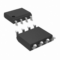
LMH6704MA/NOPB National Semiconductor, LMH6704MA/NOPB Datasheet - Page 7

LMH6704MA/NOPB
Manufacturer Part Number
LMH6704MA/NOPB
Description
IC BUFFER PROG GAIN 650MHZ 8SOIC
Manufacturer
National Semiconductor
Series
LMH®r
Datasheet
1.LMH6704MFNOPB.pdf
(12 pages)
Specifications of LMH6704MA/NOPB
Amplifier Type
Buffer
Number Of Circuits
1
Slew Rate
3000 V/µs
-3db Bandwidth
650MHz
Current - Input Bias
5µA
Voltage - Input Offset
2000µV
Current - Supply
11.5mA
Current - Output / Channel
90mA
Voltage - Supply, Single/dual (±)
8 V ~ 12 V, ±4 V ~ 6 V
Operating Temperature
-40°C ~ 85°C
Mounting Type
Surface Mount
Package / Case
8-SOIC (3.9mm Width)
For Use With
LMH730227 - BOARD EVALUATION FOR SOIC PKGLMH730165 - BOARD EVALUATIONLMH730216 - BOARD EVAL HS MONO AMP SOT23
Lead Free Status / RoHS Status
Lead free / RoHS Compliant
Output Type
-
Gain Bandwidth Product
-
Other names
*LMH6704MA
*LMH6704MA/NOPB
LMH6704MA
*LMH6704MA/NOPB
LMH6704MA
Application Information
FIGURE 1. Recommended Gain of +2 Circuit
FIGURE 2. Recommended Gain of +1 Circuit
FIGURE 3. Recommended Gain of −1 Circuit
20103603
20103605
20103604
7
GENERAL INFORMATION
The LMH6704 is a high speed current feedback Selectable
Gain Buffer (SGB), optimized for very high speed and low
distortion. With its internal feedback and gain-setting resis-
tors the LMH6704 offers excellent AC performance while
simplifying board layout and minimizing the affects of layout
related parasitic components. The LMH6704 has no internal
ground reference so single or split supply configurations are
both equally useful.
SETTING THE CLOSED LOOP GAIN
The LMH6704 is a current feedback amplifier with on-chip
R
+2, A
described in the chart below.
The gain accuracy of the LMH6704 is accurate and guaran-
teed over temperature to within
setting resistors, R
architecture takes advantage of the fact that the internal gain
setting resistors track each other well over a wide range of
temperature and process variation to keep the overall gain
constant, despite the fact that the individual resistors have
nominal temperature drifts. Therefore, using external resis-
tors in series with R
gain accuracy over temperature.
−1 V/V
+1 V/V
+2 V/V
F
GAIN A
= R
FIGURE 4. Alternate Unity Gain Configuration
V
G
= +1, or an A
= 465Ω. As such it can be configured with an A
V
Non-Inverting (Pin 3) Inverting (Pin 4)
Ground
Input Signal
Input Signal
F
and R
G
V
to change the gain will result in poor
= −1 by connecting pins 3 and 4 as
G
Input Connections
, match very well. The LMH6704
±
1%. The internal gain
Input Signal
NC (Open)
Ground
www.national.com
20103609
V
=


