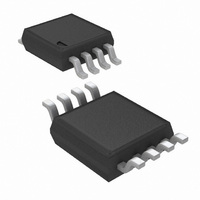
LMH6504MM/NOPB National Semiconductor, LMH6504MM/NOPB Datasheet - Page 14

LMH6504MM/NOPB
Manufacturer Part Number
LMH6504MM/NOPB
Description
IC AMP VAR GAIN LOW POWER 8MSOP
Manufacturer
National Semiconductor
Series
LMH®r
Type
Variable Gain Amplifierr
Datasheet
1.LMH6504MMNOPB.pdf
(19 pages)
Specifications of LMH6504MM/NOPB
Amplifier Type
Variable Gain
Number Of Circuits
1
Slew Rate
1500 V/µs
-3db Bandwidth
150MHz
Current - Input Bias
1.4µA
Current - Supply
11mA
Current - Output / Channel
80mA
Voltage - Supply, Single/dual (±)
7 V ~ 12 V, ±3.5 V ~ 6 V
Operating Temperature
-40°C ~ 85°C
Mounting Type
Surface Mount
Package / Case
8-MSOP, Micro8™, 8-uMAX, 8-uSOP,
Number Of Channels
1
Number Of Elements
1
Power Supply Requirement
Dual
Input Resistance
7MOhm
Input Bias Current
3.5uA
Single Supply Voltage (typ)
Not RequiredV
Dual Supply Voltage (typ)
±5V
Power Supply Rejection Ratio
65dB
Rail/rail I/o Type
No
Single Supply Voltage (min)
Not RequiredV
Single Supply Voltage (max)
Not RequiredV
Dual Supply Voltage (min)
±3.5V
Dual Supply Voltage (max)
±6V
Operating Temp Range
-40C to 85C
Operating Temperature Classification
Industrial
Mounting
Surface Mount
Pin Count
8
Package Type
MSOP
Lead Free Status / RoHS Status
Lead free / RoHS Compliant
Output Type
-
Gain Bandwidth Product
-
Voltage - Input Offset
-
Lead Free Status / Rohs Status
Compliant
Other names
LMH6504MM
LMH6504MMTR
LMH6504MMTR
Available stocks
Company
Part Number
Manufacturer
Quantity
Price
www.national.com
Application Information
LMH6504 GAIN CONTROL FUNCTION
In the plot, Gain vs. V
the control voltage. The “Gain (V/V)” plot, sometimes re-
ferred to as the S-curve, is the linear (V/V ) gain. This is a
hyperbolic tangent relationship and is given by Equation 3.
The “Gain (dB)” plots the gain in dB and is linear over a wide
range of gains. Because of this, the LMH6504 gain control is
referred to as “linear-in-dB.”
For applications where the LMH6504 will be used at the
heart of a closed loop AGC circuit, the S-curve control char-
acteristic provides a broad linear (in dB) control range with
soft limiting at the highest gains where large changes in
control voltage result in small changes in gain. For applica-
tions requiring a fully linear (in dB) control characteristic, use
the LMH6504 at half gain and below (V
AVOIDING OVERDRIVE OF THE LMH6504 GAIN
CONTROL INPUT
There is an additional requirement for the LMH6504 Gain
Control Input (V
supplies). The gain control circuitry may saturate and the
gain may actually be reduced. In applications where V
being driven from a DAC, this can easily be addressed in the
software. If there is a linear loop driving V
loop, other methods of limiting the input voltage should be
implemented. One simple solution is to place a 2.2:1 resis-
tive divider on the V
is operating off of
exceed 5V and through the divider V
IMPROVING THE LMH6504 LARGE SIGNAL
PERFORMANCE
Figure 4 illustrates an inverting gain scheme for the
LMH6504.
The input signal is applied through the R
pin should be grounded through a 25Ω resistor. The maxi-
mum gain range of this configuration is given in the following
equation:
Eq. 5
FIGURE 4. Inverting Amplifier
G
): V
±
G
5V supplies as well, its output will not
G
G
input. If the device driving this divider
, we can see the gain as a function of
must not exceed +2.3V (with
G
can not exceed 2.3V.
G
G
G
≤ 1V).
(Continued)
, such as an AGC
resistor. The V
20084354
±
G
5V
IN
is
14
The inverting slew rate of the LMH6504 is much higher than
that of the non-inverting slew rate. This 2X performance
improvement comes about because in the non-inverting con-
figuration, the slew rate of the overall amplifier is limited by
the input buffer. In the inverting circuit, the input buffer re-
mains at a fixed voltage and does not affect slew rate.
TRANSMISSION LINE MATCHING
One method for matching the characteristic impedance of a
transmission line is to place the appropriate resistor at the
input or output of the amplifier. Figure 5 shows a typical
circuit configuration for matching transmission lines.
The resistors R
istic impedance, Z
C
frequency range. It compensates for the increase of the op
amp’s output impedance with frequency.
MINIMIZING PARASITIC EFFECTS ON SMALL SIGNAL
BANDWIDTH
The best way to minimize parasitic effects is to use surface
mount components and to minimize lead lengths and com-
ponent distance from the LMH6504. For designs utilizing
through-hole components, specifically axial resistors, resis-
tor self-capacitance should be considered. Example: the
average magnitude of parasitic capacitance of RN55D 1%
metal film resistors is about 0.15 pF with variations of as
much as 0.1 pF between lots. Given the LMH6504’s ex-
tended bandwidth, these small parasitic reactance variations
can cause measurable frequency response variations in the
highest octave. We therefore recommend the use of surface
mount resistors to minimize these parasitic reactance ef-
fects.
RECOMMENDATIONS
Here are some recommendations to avoid problems and to
get the best performance:
• Do not place a capacitor across R
• Keep traces connecting R
• Place a small resistor (20-50Ω) between the output and
• Cut away the ground plane, if any, under R
• Keep decoupling capacitors as close as possible to the
• Connect pin 2 through a minimum resistance of 25Ω.
O
priately chosen series RC combination could be used to
shape the frequency response.
possible
C
LMH6504.
to match the output transmission line over a greater
L
FIGURE 5. TRANSMISSION LINE MATCHING
S
, R
O
I
, R
, of the transmission line or cable. Use
O
, and R
F
T
separated and as short as
are equal to the character-
F
. However, an appro-
G
20084356


