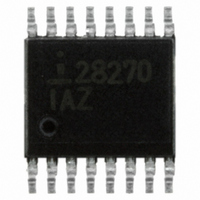
ISL28270IAZ-T13 Intersil, ISL28270IAZ-T13 Datasheet - Page 16

ISL28270IAZ-T13
Manufacturer Part Number
ISL28270IAZ-T13
Description
IC INSTR AMP RRIO DUAL 16-QSOP
Manufacturer
Intersil
Datasheet
1.ISL28470EVAL1Z.pdf
(18 pages)
Specifications of ISL28270IAZ-T13
Amplifier Type
Instrumentation
Number Of Circuits
2
Output Type
Rail-to-Rail
Slew Rate
0.5 V/µs
-3db Bandwidth
240kHz
Current - Input Bias
500pA
Voltage - Input Offset
35µV
Current - Supply
120µA
Current - Output / Channel
29mA
Voltage - Supply, Single/dual (±)
2.4 V ~ 5.5 V, ±1.2 V ~ 2.75 V
Operating Temperature
-40°C ~ 125°C
Mounting Type
Surface Mount
Package / Case
16-QSOP
Lead Free Status / RoHS Status
Lead free / RoHS Compliant
Gain Bandwidth Product
-
Other names
ISL28270IAZ-T13TR
the in-amp maintains constant differential voltage across the
input terminals and feedback terminals (FB- - FB+) =
(IN+ - IN-), the transfer function of Figure 51 can be derived
from Equation 3. Note that the VREF gain term is eliminated,
and susceptibility to external noise is reduced.
A finite resistance R
an output offset of VIN*(R
approaches zero, Equation 3 is simplified to Equation 4 for
Figure 51. VOUT is simply shifted by an amount VREF.
External Resistor Mismatches
Because of the independent pair of feedback terminals
provided by the in-amps, the CMRR is not degraded by any
resistor mismatches. Hence, unlike a three op amp and
especially a two op amp in-amp realization, the ISL28270,
ISL28273 and ISL28470 reduce the cost of external
components by allowing the use of 1% or more tolerance
resistors without sacrificing CMRR performance. The CMRR
will be typically 110dB regardless of the tolerance of the
resistors used. Instead, a resistor mismatch results in a
higher deviation from the theoretical gain - gain error.
Gain Error and Accuracy
The gain error indicated in the “Electrical Specifications”
table on page 4 is the inherent gain error alone. The gain
error specification listed does not include the gain error
contributed by the resistors. There is an additional gain error
due to the tolerance of the resistors used. The resulting
non-ideal transfer function effectively becomes: (see
Equation 5)
VOUT
VOUT
VOUT
VIN
FIGURE 51. REFERENCE CONNECTION WITH AN AVAILABLE
VCM
VREF
=
R
IN+ IN-
=
=
=
S
IN+
IN-
⎛
⎜
⎝
⎛
⎜
⎝
1
1
1
–
+
+
+
VREF
R
--------------------- -
------- -
R
------- -
R
R
R
S
G
G
F
F
R
⎞
⎟
⎠
⎞
⎟
⎠
R
+
G
(
G
×
VIN
R
[
F
S
1
in series with the VREF source, adds
±
)
+
+
(
VREF
E
(
S
VREF
RG
/R
FB+
FB-
IN+
IN-
16
G
+
). As the series resistance R
2.4V TO 5.5V
E
+
+
)
-
-
RF
R
F
+
V+
V-
E
(ISL28270, ISL28470)
G
)
]
×
VIN
ISL28270, ISL28273, ISL28470
(EQ. 3)
(EQ. 4)
(EQ. 5)
VOUT
S
Where:
E
E
E
The term [1 - (E
theoretical gain. Thus, (E
error. For example, if 1% resistors are used, the total gain
error would be shown in Equation 6.
Disable/Power-Down
The ISL28270 and ISL28470 have an enable/disable pin for
each channel. They can be powered down to reduce the
supply current to typically 4µA when all channels are off.
When disabled, the corresponding output is in a high
impedance state. The active low EN pin has an internal pull
down and hence can be left floating and the in-amp enabled
by default. When the EN is connected to an external logic,
the in-amp will shutdown when EN pin is pulled above 2V,
and will power up when EN bar is pulled below 0.8V.
Unused Channels
The ISL28270, ISL28273 and ISL28470 are dual and quad
channel op amps. If the application only requires one
channel when using the ISL28270, ISL28273 or less than 4
channels when using the ISL28470, the user must configure
the unused channel(s) to prevent them from oscillating. The
unused channel(s) will oscillate if the input and output pins
are floating. This will result in higher than expected supply
currents and possible noise injection into the channel being
used. The proper way to prevent this oscillation is to short
the IN+ and IN- terminals to ground and short the FB+, FB-
and the output terminals to ground as shown in Figure 52.
TotalGainError
TotalGainError
RG
RF
G
FIGURE 52. PREVENTING OSCILLATIONS IN UNUSED
= Tolerance of RG
= Tolerance of RF
= Gain Error of the ISL28270
CHANNELS
RG
=
=
±
±
+E
(
(
FB+
E
0.01
FB-
IN+
IN-
RG
RF
+
+
RG
+
+
-
+E
-
0.01
E
RF
G
+E
)] is the deviation from the
+
+
RF
0.005
E
G
+E
(
typical
)
G
=
) is the total gain
1/2 ISL28270, ISL28273
1/4 ISL28470
±
2.5%
)
)
October 21, 2009
(EQ. 6)
FN6260.6


