LMC6482IN/NOPB National Semiconductor, LMC6482IN/NOPB Datasheet

IC OP AMP DUAL CMOS R-R 8-DIP

LMC6482IN/NOPB

Manufacturer Part Number
LMC6482IN/NOPB
Description
IC OP AMP DUAL CMOS R-R 8-DIP
Manufacturer
National Semiconductor
Datasheets

Specifications of LMC6482IN/NOPB

Amplifier Type
General Purpose
Number Of Circuits
2
Output Type
Rail-to-Rail
Slew Rate
1.3 V/µs
Gain Bandwidth Product
1.5MHz
Current - Input Bias
0.02pA
Voltage - Input Offset
110µV
Current - Supply
1.3mA
Current - Output / Channel
30mA
Voltage - Supply, Single/dual (±)
3 V ~ 15.5 V, ±1.5 V ~ 7.75 V
Operating Temperature
-40°C ~ 85°C
Mounting Type
Through Hole
Package / Case
8-DIP (0.300", 7.62mm)
Bandwidth
1.5 MHz
Channel Separation
150
Common Mode Rejection Ratio
82
Current, Input Bias
0.02 pA
Current, Input Offset
0.01 pA
Current, Output
30 mA
Current, Supply
1.3 mA
Harmonic Distortion
0.01 %
Impedance, Thermal
90 °C/W
Number Of Amplifiers
Dual
Package Type
MDIP-8
Resistance, Input
10 Teraohms
Temperature, Operating, Range
-40 to +85 °C
Voltage, Gain
666 V/mV
Voltage, Input
3 to 15.5 V
Voltage, Noise
37 nV/sqrt Hz
Voltage, Offset
0.11 mV
Voltage, Output, High
14.7 V
Voltage, Output, Low
0.16 V
Voltage, Supply
5 V
Lead Free Status / RoHS Status
Lead free / RoHS Compliant
-3db Bandwidth
-
Lead Free Status / Rohs Status
RoHS Compliant part Electrostatic Device
Other names
*LMC6482IN
*LMC6482IN/NOPB
LMC6482IN
© 2004 National Semiconductor Corporation
LMC6482
CMOS Dual Rail-To-Rail Input and Output Operational
Amplifier
General Description
The LMC6482 provides a common-mode range that extends
to both supply rails. This rail-to-rail performance combined
with excellent accuracy, due to a high CMRR, makes it
unique among rail-to-rail input amplifiers.
It is ideal for systems, such as data acquisition, that require
a large input signal range. The LMC6482 is also an excellent
upgrade for circuits using limited common-mode range am-
plifiers such as the TLC272 and TLC277.
Maximum dynamic signal range is assured in low voltage
and single supply systems by the LMC6482’s rail-to-rail out-
put swing. The LMC6482’s rail-to-rail output swing is guar-
anteed for loads down to 600Ω.
Guaranteed low voltage characteristics and low power dis-
sipation make the LMC6482 especially well-suited for
battery-operated systems.
LMC6482 is also available in MSOP package which is al-
most half the size of a SO-8 device.
See the LMC6484 data sheet for a Quad CMOS operational
amplifier with these same features.
3V Single Supply Buffer Circuit
Connection Diagram
Rail-To-Rail Input
01171301
DS011713
Features
(Typical unless otherwise noted)
n Rail-to-Rail Input Common-Mode Voltage Range
n Rail-to-Rail Output Swing (within 20mV of supply rail,
n Guaranteed 3V, 5V and 15V Performance
n Excellent CMRR and PSRR: 82dB
n Ultra Low Input Current: 20fA
n High Voltage Gain (R
n Specified for 2kΩ and 600Ω loads
n Available in MSOP Package
Applications
n Data Acquisition Systems
n Transducer Amplifiers
n Hand-held Analytic Instruments
n Medical Instrumentation
n Active Filter, Peak Detector, Sample and Hold, pH
n Improved Replacement for TLC272, TLC277
(Guaranteed Over Temperature)
100kΩ load)
Meter, Current Source
01171302
01171304
L
= 500kΩ): 130dB
Rail-To-Rail Output
01171303

Related parts for LMC6482IN/NOPB

LMC6482IN/NOPB Summary of contents

Page 1

... See the LMC6484 data sheet for a Quad CMOS operational amplifier with these same features. 3V Single Supply Buffer Circuit Rail-To-Rail Input 01171301 Connection Diagram © 2004 National Semiconductor Corporation Features (Typical unless otherwise noted) n Rail-to-Rail Input Common-Mode Voltage Range (Guaranteed Over Temperature) n Rail-to-Rail Output Swing (within 20mV of supply rail, 100kΩ ...

Page 2

... Absolute Maximum Ratings If Military/Aerospace specified devices are required, please contact the National Semiconductor Sales Office/ Distributors for availability and specifications. ESD Tolerance (Note 2) Differential Input Voltage Voltage at Input/Output Pin (V + − Supply Voltage (V − Current at Input Pin (Note 12) Current at Output Pin (Notes 3, 8) ...

Page 3

DC Electrical Characteristics Unless otherwise specified, all limits guaranteed for T limits apply at the temperature extremes. Symbol Parameter + V Output Swing ...

Page 4

AC Electrical Characteristics Unless otherwise specified, all limits guaranteed for T limits apply at the temperature extremes. Symbol Parameter T.H.D. Total Harmonic Distortion DC Electrical Characteristics Unless otherwise specified, all limits guaranteed for T Symbol Parameter V Input Offset Voltage ...

Page 5

AC Electrical Characteristics Note 3: Applies to both single-supply and split-supply operation. Continuous short circuit operation at elevated ambient temperature can result in exceeding the maximum allowed junction temperature of 150˚C. Output currents in excess of Note 4: The maximum ...

Page 6

Typical Single-Supply Applications FIGURE 25. Rail-to-Rail Single Supply Low Pass Filter The low pass filter circuit in Figure 25 can be used as an anti-aliasing filter with the same voltage supply as the A/D converter. Filter designs can also take ...

Page 7

Physical Dimensions inches (millimeters) unless otherwise noted Order Package Number LMC6482AIM, LMC6482AIMX, LMC6482IM or LMC6482IMX 8-Pin Ceramic Dual-In-Line Package Order Number LMC6482AMJ/883 NS Package Number J08A 8-Pin Small Outline Package NS Package Number M08A 23 ...

Page 8

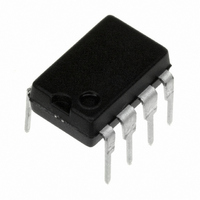
Physical Dimensions inches (millimeters) unless otherwise noted (Continued) Order Package Number LMC6482AIN, LMC6482IN 8-Lead Mini Small Outline Molded Package, JEDEC Order Number LMC6482IMM, or LMC6482IMMX 8-Pin Molded Dual-In-Line Package NS Package Number N08E NS Package Number MUA08A 24 ...

Related keywords