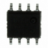
LMC6482IM/NOPB National Semiconductor, LMC6482IM/NOPB Datasheet - Page 5

LMC6482IM/NOPB
Manufacturer Part Number
LMC6482IM/NOPB
Description
IC OP AMP DUAL CMOS R-R 8-SOIC
Manufacturer
National Semiconductor
Datasheet
1.LMC6482IMNOPB.pdf
(25 pages)
Specifications of LMC6482IM/NOPB
Amplifier Type
General Purpose
Number Of Circuits
2
Output Type
Rail-to-Rail
Slew Rate
1.3 V/µs
Gain Bandwidth Product
1.5MHz
Current - Input Bias
0.02pA
Voltage - Input Offset
110µV
Current - Supply
1.3mA
Current - Output / Channel
30mA
Voltage - Supply, Single/dual (±)
3 V ~ 15.5 V, ±1.5 V ~ 7.75 V
Operating Temperature
-40°C ~ 85°C
Mounting Type
Surface Mount
Package / Case
8-SOIC (3.9mm Width)
Lead Free Status / RoHS Status
Lead free / RoHS Compliant
-3db Bandwidth
-
Other names
*LMC6482IM
*LMC6482IM/NOPB
LMC6482IM
*LMC6482IM/NOPB
LMC6482IM
Available stocks
Company
Part Number
Manufacturer
Quantity
Price
Company:
Part Number:
LMC6482IM/NOPB
Manufacturer:
TI
Quantity:
3 000
Part Number:
LMC6482IM/NOPB
Manufacturer:
NS/国半
Quantity:
20 000
AC Electrical Characteristics
Note 3: Applies to both single-supply and split-supply operation. Continuous short circuit operation at elevated ambient temperature can result in exceeding the
maximum allowed junction temperature of 150˚C. Output currents in excess of
Note 4: The maximum power dissipation is a function of T
− T
Note 5: Typical Values represent the most likely parametric norm.
Note 6: All limits are guaranteed by testing or statistical analysis.
Note 7: V
Note 8: Do not short circuit output to V
Note 9: V
Note 10: Input referred, V
Note 11: Connected as voltage Follower with 2V step input. Number specified is the slower of either the positive or negative slew rates.
Note 12: Limiting input pin current is only necessary for input voltages that exceed absolute maximum input voltage ratings.
Note 13: Guaranteed limits are dictated by tester limitations and not device performance. Actual performance is reflected in the typical value.
Note 14: For guaranteed Military Temperature parameters see RETS6482X.
Typical Performance Characteristics
specified
V
A
S
)/θ
= +15V, Single Supply, T
JA
. All numbers apply for packages soldered directly into a PC board.
+
+
= 15V, V
= 15V. Connected as Voltage Follower with 10V step input. Number specified is the slower of either the positive or negative slew rates.
Sourcing Current vs. Output Voltage
Supply Current vs. Supply Voltage
CM
= 7.5V and R
+
= 15V and R
L
A
connected to 7.5V. For Sourcing tests, 7.5V ≤ V
+
= 25˚C unless otherwise
, when V
L
= 100 kΩ connected to 7.5V. Each amp excited in turn with 1 kHz to produce V
+
is greater than 13V or reliability will be adversely affected.
J(max)
01171340
01171342
, θ
(Continued)
JA
, and T
A
. The maximum allowable power dissipation at any ambient temperature is P
±
5
30mA over long term may adversely affect reliability.
O
≤ 11.5V. For Sinking tests, 3.5V ≤ V
Sourcing Current vs. Output Voltage
Input Current vs. Temperature
O
= 12 V
O
≤ 7.5V.
PP
.
01171343
01171341
www.national.com
D
= (T
J(max)


